Solder Reflow: An In-Depth Guide to the Process and Techniques
This article provides a detailed overview of the solder reflow process, types of reflow ovens, temperature profiles, solder paste composition and selection, reflow process potential challenges, solutions, inspection, and quality control techniques.

25 May, 2023. 23 minutes read
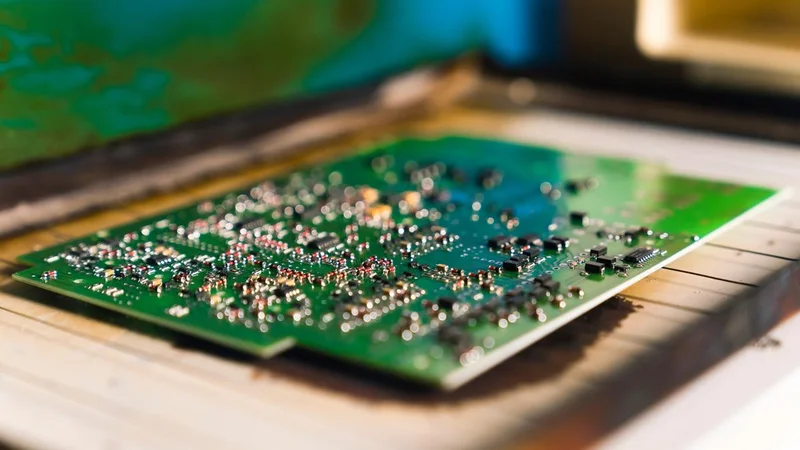
Reflow soldering furnace used on mounted PCB
Introduction
Solder reflow is a critical process in the electronics industry, primarily used to attach surface-mount components to printed circuit boards (PCBs). It involves applying solder paste to specific locations on a PCB, placing the components on the paste, and then heating the assembly in a reflow oven. The solder paste melts, forming a reliable electrical and mechanical connection between the component and the PCB. The quality of these connections has a significant impact on the performance and reliability of the final electronic product.
During the solder reflow process, various factors influence the quality of the solder joint, including the solder paste's composition, the type of reflow oven, and the temperature profile. Understanding these factors and how they interact is essential for achieving optimal soldering results. This article will dive deep into the solder reflow process, exploring its different aspects, challenges, and best practices. It will provide a comprehensive understanding of the techniques and principles involved, enabling the reader to make informed decisions when working with solder reflow. [1]
Solder Reflow Process Overview
Preparing the PCB
To ensure high-quality solder joints, thorough Proper PCB cleaning is essential before solder reflow to ensure high-quality solder joints. The cleanliness of the PCB surface directly affects the solder paste's ability to adhere to the board and form a reliable connection. Contamination, such as dust, grease, and oxidation, can lead to soldering defects and decreased product reliability.
Several methods can be used to clean PCBs before solder reflow, including ultrasonic cleaning, aqueous cleaning, and solvent cleaning. Ultrasonic cleaning uses high-frequency sound waves to remove contaminants. Aqueous cleaning relies on water-based solutions, while solvent cleaning uses specialized chemicals to dissolve contaminants. Each method has advantages and disadvantages, depending on factors such as the type and degree of contamination, PCB material, and environmental considerations.
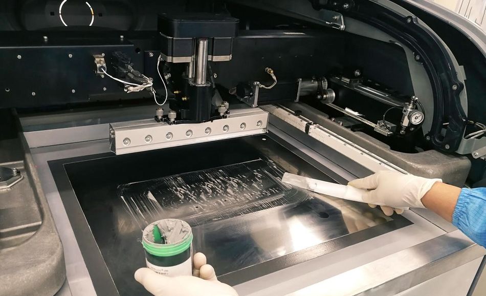
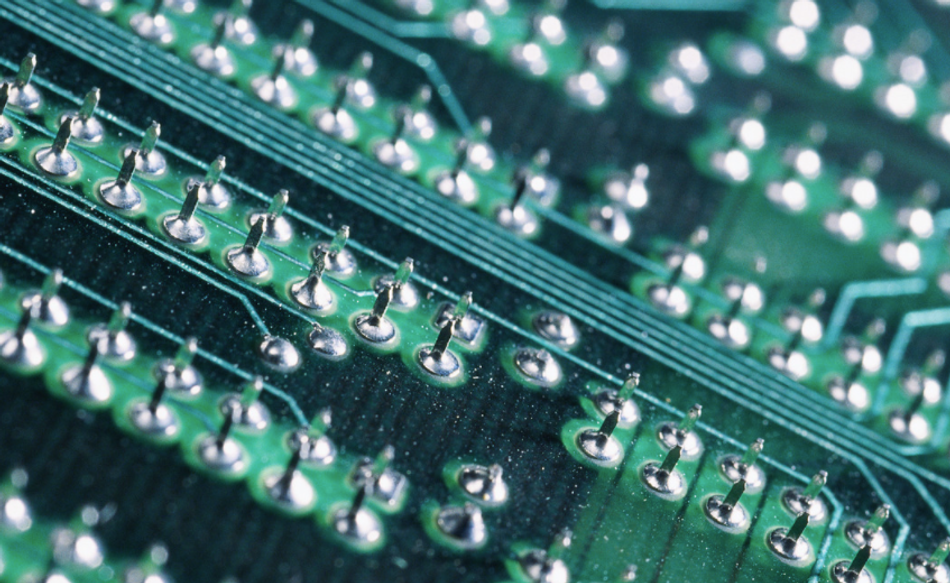
After the PCB is cleaned, the next step is to apply solder paste. Solder paste is a mixture of metal alloy particles, flux, and other additives that melt during reflow. This creates a bond between the PCB pads and component terminals. A critical aspect of solder paste application is the accurate deposition of the paste onto the PCB pads. This is typically achieved using a stencil printer.
Stencil Printing
Stencil printing is a crucial step in the solder reflow process, as it ensures accurate solder paste deposition onto the PCB pads. A well-designed stencil is essential for achieving optimal solder joint quality. Stencils are typically made from stainless steel or polyimide film and have apertures that match the PCB pad layout. The stencil is placed on the PCB, and solder paste is spread across it using a squeegee, filling the apertures and transferring the paste to the pads. [2]
Several factors influence the stencil printing process and the quality of solder paste deposition:
Stencil design: The thickness and aperture dimensions of the stencil must be precisely matched to the PCB pad size and component requirements. The thickness of the stencil determines the amount of solder paste deposited on the pads, while the aperture dimensions control the paste's lateral spread. A well-designed stencil minimizes the risk of solder bridging and insufficient solder on the pads.
The formula to calculate the approximate thickness of the PCB stencil is stated below:
Area Ratio = Area of the pad / Area of the aperture walls = L * W / 2 * (L + W) * T
Where, L = Length of Pad, W = Width of Pad, T = Thickness of Pad
Printing parameters: The squeegee angle, pressure, and speed play a significant role in stencil printing. An incorrect squeegee angle can lead to incomplete aperture filling, while excessive pressure or speed may cause smearing or misalignment of the solder paste on the pads. Proper calibration and adjustment of these parameters ensure accurate solder paste deposition.
Solder paste properties: The solder paste's rheological properties, such as viscosity and thixotropy, affect its ability to flow through the stencil apertures and adhere to the PCB pads. Solder paste must have a suitable viscosity and thixotropic behavior for consistent and accurate deposition. The paste's metal content, alloy composition, and particle size distribution are critical factors influencing the final solder joint quality.
Regular inspection and maintenance of the stencil printer are necessary to prevent defects and maintain high-quality solder paste deposition. This includes cleaning the stencil to remove solder paste residue and checking the alignment and accuracy of the printing process.
Pick and Place
The pick and place process is essential in the solder reflow process, where surface mount components are accurately placed on the PCB pads coated with solder paste. Pick and place machines, also known as component placement systems, are responsible for this task. These machines use a combination of cameras, robotic arms, and vacuum nozzles to pick up components from the component reels or trays and accurately place them on the PCB.
Several factors contribute to the efficiency and accuracy of the pick and place process:
Component recognition and orientation: Modern pick and place machines use advanced vision systems to recognize components, determine their orientation, and ensure proper placement on the PCB. These vision systems can detect various component types, including passive components, integrated circuits, and connectors. The vision system's accuracy is crucial for avoiding placement errors such as tombstoning, skewing, and misalignment.
Placement speed: The speed at which the machine can pick up components and place them on the PCB is critical in determining the production throughput. High-speed placement machines can place tens of thousands of components per hour, while more flexible machines may have a lower placement rate but support a wider range of component types and sizes.
Machine accuracy and repeatability: The precision of the pick and place machine determines the placement accuracy of the components on the PCB. High-precision machines can place components with an accuracy of a few microns, ensuring reliable solder joints and minimal defects during the reflow process. Repeatability is the machine's ability to consistently place components within a specified accuracy range, essential for maintaining high-quality solder joints across multiple PCB assemblies.
Feeder capacity and changeover time: The number of component feeders a machine can accommodate directly impacts the machine's versatility and productivity. Machines with more feeder slots can handle many different components, reducing the need for frequent changeovers. Additionally, machines with quick changeover times minimize production downtime, increasing overall efficiency.
Proper calibration and maintenance of the pick and place machine are vital for ensuring accurate component placement and minimizing defects during the solder reflow process.
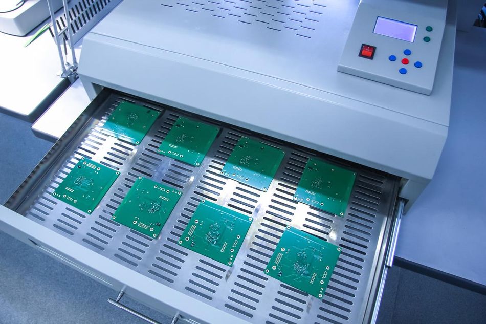
Solder Reflow Oven
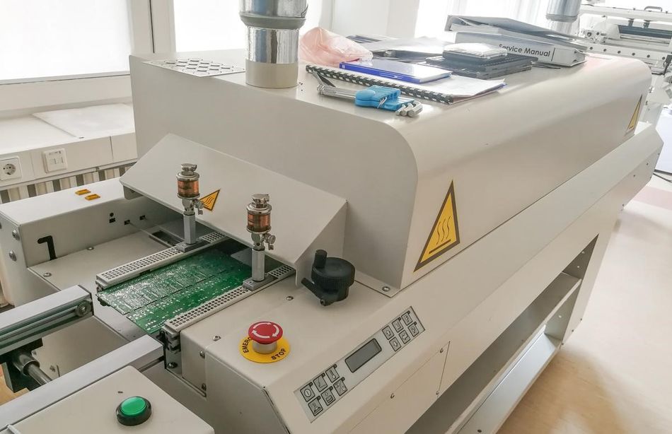
Solder reflow ovens are the equipment used to heat the solder paste and create a solid connection between soldered surface-mount components and the PCB. They use controlled temperature profiles to achieve optimal solder joint quality and reliability. The reflow process consists of four main phases: preheating, soaking, reflow, and cooling. Each phase is critical to achieving a high-quality solder joint and preventing solder-related defects.
During the preheating phase, the oven gradually raises the temperature of the PCB assembly to prevent thermal shock and damage to the components. The soaking phase ensures that the entire PCB reaches a uniform temperature, allowing the flux in the solder paste to activate and remove oxides from the surfaces to be soldered.
The reflow phase is when the oven reaches its maximum temperature, causing the solder paste to melt and form a strong metallurgical bond between the component leads and the PCB pads. The range for reflow temperature is between 240 and 250 degrees Celsius for a Pb-free (Sn/Ag) solder. Finally, the cooling phase rapidly lowers the temperature to solidify the solder joints and prevent the formation of intermetallic compounds that could weaken the solder connection.
Types of Reflow Ovens
Several types of reflow ovens are available in the market, each with its own advantages and disadvantages. The two main types are infrared (IR) ovens and convection ovens.
Infrared (IR) Ovens: Infrared ovens heat the PCB assembly using infrared radiation. This highly efficient heating method directly transfers energy to the solder paste and components, resulting in a rapid heating process. However, IR ovens can cause uneven heating due to the absorption characteristics of different materials, which may lead to temperature variations across the PCB assembly. Infrared ovens are typically less expensive than convection ovens but are less commonly used in modern electronics manufacturing due to the potential for uneven heating.
Convection Ovens: Convection ovens use heated air to transfer heat to the PCB assembly. These ovens can be further classified into two subcategories: forced air convection and vapor phase reflow ovens. Forced air convection ovens to use fans to circulate hot air around the PCB assembly, providing uniform heating and minimizing the risk of temperature variations. Vapor phase reflow ovens use a heat transfer medium, such as a specialized liquid with a high boiling point, to heat the PCB assembly evenly. When the liquid vaporizes, it transfers heat to the PCB assembly, resulting in a highly controlled and uniform heating process. Convection ovens are generally more expensive than IR ovens but provide superior temperature control and even heating, making them the preferred choice for modern electronics manufacturing. [3]
A suitable reflow oven selection depends on factors such as production volume, budget, and specific process requirements. Proper calibration and maintenance of the reflow oven are critical to ensuring optimal solder joint quality and minimizing solder-related defects.
Reflow Oven Zones
Reflow ovens are typically divided into a series of zones, each with independently controlled temperature settings. The arrangement of these zones plays a critical role in achieving a precise and uniform temperature profile throughout the reflow process. A typical reflow oven consists of the following zones:
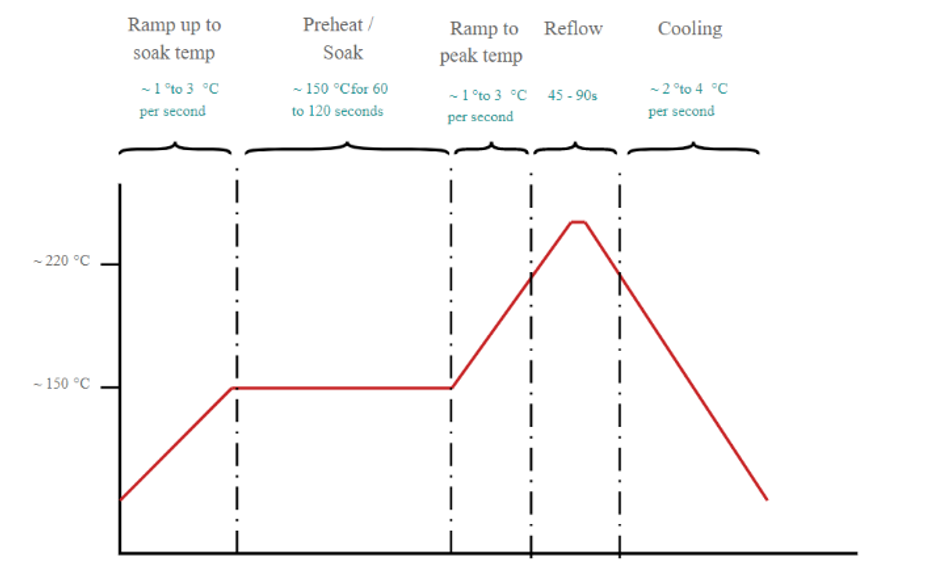
Preheating Zone: The preheating zone is the first zone in the reflow oven and is responsible for gradually raising the temperature of the PCB assembly. This process helps prevent thermal shock, which could damage sensitive components. The rate at which the temperature increases in this zone is crucial, as too rapid heating could cause component warping, while too slow heating could lead to solder paste drying. An ideal preheat rate is between 1 and 3°C per second.
Soaking Zone: The temperature is held constant in the soaking zone, allowing the PCB assembly to reach a uniform temperature. This phase ensures that the flux in the solder paste activates and removes oxides from the surfaces to be soldered. The soaking zone is vital for achieving consistent solder joint quality, as it helps minimize temperature variations across the PCB assembly.
Reflow Zone: The reflow zone is where the peak temperature is reached, causing the solder paste to melt and form a strong metallurgical bond between the component leads and the PCB pads. The peak temperature typically ranges between 235°C and 250°C, depending on the solder paste used. Maintaining this temperature within a specified range and duration is essential to ensure optimal solder joint formation without damaging components or causing other solder-related defects.
Cooling Zone: The cooling zone is the final zone in the reflow oven, where the temperature is rapidly lowered to solidify the solder joints. A controlled cooling rate is critical to prevent the formation of intermetallic compounds that could weaken the solder connection. Too rapid cooling can cause thermal soak, while too slow cooling can lead to the formation of brittle solder joints. An ideal cooling rate is between 2 and 4°C per second.
The number of zones in a reflow oven can vary depending on the specific model and manufacturer. More advanced reflow ovens may have additional zones or sub-zones for fine-tuning the temperature profile, providing increased control over the reflow process and ensuring consistent solder joint quality.
Temperature Profiles
A temperature profile is a critical aspect of the reflow soldering process, as it influences the quality and reliability of the solder joints. It represents the temperature changes experienced by the PCB assembly throughout the reflow oven zones. The right temperature profile is essential to ensure optimal solder joint formation and minimize solder-related defects. [4]
Ramp-Soak-Spike (RSS) Profile: The Ramp-Soak-Spike (RSS) profile is a common temperature profile used in reflow soldering. In this profile, the temperature ramps up during the preheating zone, followed by a constant temperature (soak) phase in the soaking zone. Finally, the temperature spikes to its peak in the reflow zone before cooling down. The RSS profile ensures that the PCB assembly and its components experience a controlled temperature change, preventing thermal soak and reducing the risk of defects such as solder bridging and voids.
Ramp-to-Spike (RTS) Profile: The Ramp-to-Spike (RTS) profile is another temperature profile often used in reflow soldering. In this profile, the temperature continuously increases from the preheating zone until it reaches its peak in the reflow zone. There is no distinct soaking phase in this profile. RTS is typically employed for lead-free soldering processes, allowing for a more rapid heating rate to accommodate the higher melting point of lead-free solder alloys.
Custom Profiles: Custom temperature profiles can be developed based on the specific requirements of the PCB assembly and the solder paste used. Factors that influence the choice of a custom profile include the complexity of the PCB, component density, component types, and the thermal properties of the solder paste. Custom profiles provide more precise control over the reflow process, enabling better solder joint quality and minimizing defects.
To achieve the desired temperature profile, the reflow oven must be accurately calibrated and its heating elements adjusted accordingly. Periodic thermal profiling is recommended to ensure that the reflow oven maintains its performance and provides consistent solder joint quality. Thermal profiling involves measuring the temperature experienced by the PCB assembly at various points throughout the reflow process, using thermocouples attached to the PCB or a dedicated profiling board. The gathered data can then be used to fine-tune the reflow oven settings and optimize the temperature profile. [5]
Solder Paste
Solder paste is a vital material in the reflow soldering process, as it forms the electrical and mechanical connections between the components and the PCB. It consists of tiny solder particles suspended in a flux medium, which helps to clean the surfaces to be soldered, improves wetting, and prevents oxidation during the soldering process.
Composition
Solder paste primarily comprises two main components: solder alloy and flux. The specific composition of solder paste depends on the application requirements and the type of solder alloy being used.
Solder Alloy: The solder alloy is made up of tiny metal particles, usually in the range of 20-50 microns in diameter. The alloy composition determines the solder joints' melting point, wetting properties, and mechanical strength. Common solder alloys include tin-lead (SnPb) and lead-free alternatives such as tin-silver-copper (SAC). The choice of the alloy depends on factors such as the required operating temperature, environmental considerations, and regulatory requirements.
Flux: The flux is a chemically active medium that surrounds the solder particles and serves multiple purposes during reflow. It helps to remove any oxide layers present on the surfaces to be soldered, promotes wetting of the solder, and prevents further oxidation during the soldering iron process. Fluxes can be classified into three categories based on their activity level: low, medium, and high. The choice of flux depends on factors such as the surface oxidation level, the solder alloy type, and the desired solder joint quality.
In addition to the primary components, solder paste may contain additives, such as rheological modifiers, to improve printability and stability and surfactants to enhance wetting properties. The specific composition of a solder paste must be tailored to the requirements of the reflow soldering process, considering factors such as the type of components, PCB material, and the thermal profile of the reflow oven.
Solder Paste Selection
Selecting the appropriate solder paste for a specific application is critical for achieving optimal soldering performance, high yield, and long-term reliability of the resulting electronic assemblies. Several factors must be considered when selecting a solder paste:
Type of Solder Alloy: The choice of solder alloy is a crucial factor in the solder paste selection. Tin-lead (SnPb) alloys have been widely used in the electronics industry due to their excellent solderability, low cost, and ease of use. However, environmental concerns and regulations have driven the adoption of lead-free solder alloys, such as tin-silver-copper (SAC), which exhibit higher melting points and different wetting characteristics than SnPb alloys.
Flux Activity Level: The flux activity level in the solder paste should be selected based on the degree of surface oxidation and the required solder joint quality. A higher activity level flux may be necessary for oxidized surfaces or critical applications where high joint quality is essential. Conversely, a low activity level flux may suit less demanding applications with clean surfaces.
Particle Size Distribution: The particle size distribution of the solder alloy affects the printability, reflow performance, and voiding characteristics of the solder paste. Smaller particle sizes generally offer better printability and reduced voiding but may be more prone to oxidation and handling issues. Commonly used particle size distributions in solder paste include Type 3 (25-45 microns) and Type 4 (20-38 microns).
Viscosity and Rheology: The viscosity and rheological properties of the solder paste should be compatible with the stencil printing process and equipment used. To achieve consistent and precise deposition onto the PCB, the paste must exhibit appropriate flow and thixotropic behavior.
Thermal Stability: The solder paste must have adequate thermal stability to withstand the reflow soldering process's temperature profile. This includes resistance to premature flux activation, solder balling, and slump.
Compatibility with Components and PCB Materials: The solder paste should be compatible with the materials used in the components and PCB, as well as any surface finishes, to prevent issues such as de-wetting, solder joint embrittlement, and intermetallic compound formation.
To ensure optimal performance, evaluating and testing the selected solder paste under actual mass production conditions, including stencil printing, component placement, and reflow soldering processes, is essential. This will help identify potential issues and fine-tune the process parameters to achieve the best soldering results.
Reflow Process Challenges and Solutions
Tombstoning
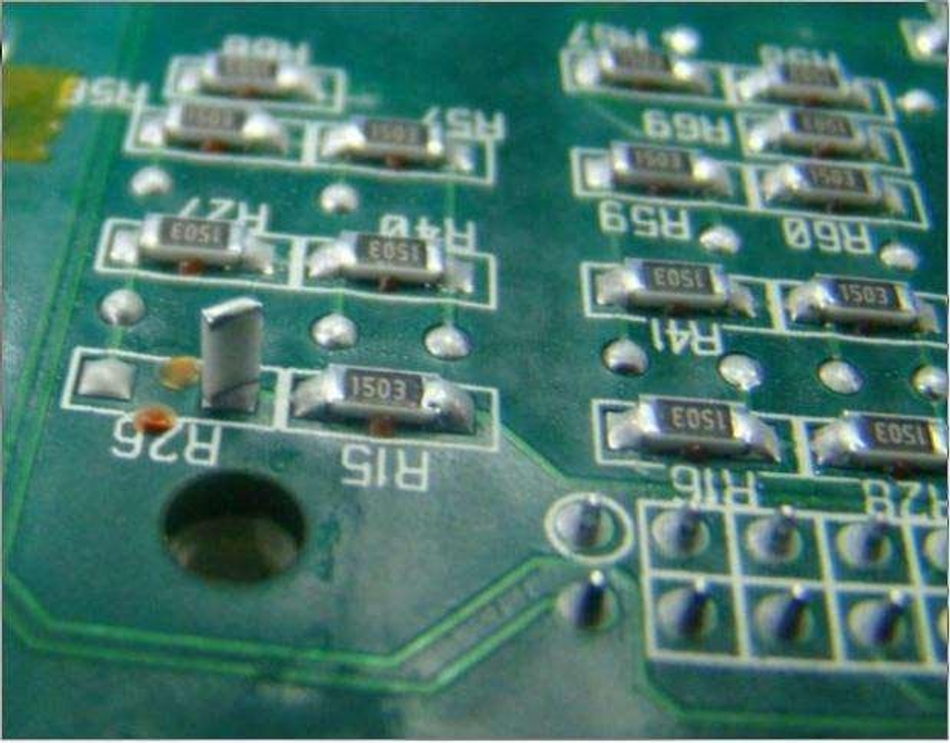
Tombstoning, also known as the Manhattan effect or drawbridging, is a common soldering defect that occurs during the reflow process when a surface-mounted component, typically a chip resistor or capacitor, lifts from one end and stands vertically on the PCB. This results in an open circuit and can lead to a malfunctioning electronic assembly.
Several factors contribute to the occurrence of tombstoning:
Uneven Heating: If one side of the component reaches the solder's melting point faster than the other side, the molten solder's surface tension can pull the component into a vertical position. Ensuring that the reflow oven's temperature profile is uniform and matches the solder paste and component specifications can help mitigate this issue.
Uneven Wetting: Different wetting rates on each end of the component can also cause tombstoning. Factors influencing wetting rates include component and pad geometries, solder paste composition, and the PCB's surface finish. To address this issue, it is essential to optimize the stencil design, select the appropriate solder paste, and ensure consistent surface finishes on the PCB.
Component and Pad Misalignment: Misaligned components or pads can lead to uneven solder distribution, increasing the likelihood of tombstoning. Accurate placement of components during the pick-and-place process and proper pad design are critical to reducing the occurrence of this defect.
Pad and Component Size: Using components with larger body sizes or wider terminations can help increase the component's stability during the reflow process, reducing the risk of tombstoning. Furthermore, ensuring that pad sizes are compatible with the selected components can help maintain a balanced solder distribution.
To minimize the occurrence of tombstoning, it is essential to understand and control the factors contributing to this defect. Implementing a robust quality assurance program, monitoring the reflow process, and refining process parameters based on feedback can significantly reduce the occurrence of tombstoning and improve the reliability of the resulting electronic assemblies.
Voids
Voids are air pockets or gas-filled gaps within the solder joint during reflow. They can adversely affect the electrical and thermal performance of the joint, leading to reduced reliability and potential failures in electronic assemblies. Voids can occur in solder joints but are most commonly found in a ball grid array (BGA) and quad flat no-lead (QFN) packages.
Causes of Voids: Several factors contribute to the formation of voids:
Outgassing: Gases generated during the reflow process, either from the solder paste or the components themselves, can become trapped within the solder joint. This can occur if the gas cannot escape due to inadequate venting or excessive solder paste viscosity.
Oxidation: The presence of oxide layers on component leads, pads, or solder balls can impede proper wetting, creating gaps within the solder joint. Proper storage and handling of solder paste and components can help minimize oxidation-related voids.
Solder Paste Handling and Storage: Improper handling or storage of solder paste, such as exposure to humidity or temperature fluctuations, can cause changes in paste viscosity and consistency, leading to void formation. Ensuring that solder paste is stored according to manufacturer guidelines can help reduce voids.
Solutions for Void Reduction: Implementing various process modifications can help reduce the occurrence of voids:
Optimizing the Reflow Profile: Adjusting the reflow oven temperature profile to provide a gradual ramp-up in temperature and sufficient time above the solder's melting point allows gases to escape more effectively, reducing the likelihood of void formation.
Solder Paste Selection: Choosing a solder paste with low voiding characteristics, such as low-voiding formulations or solder pastes with appropriate flux chemistries, can help minimize voids.
Stencil Design and Printing: Ensuring proper stencil design, such as aperture size and shape, and maintaining consistent solder paste printing can result in more uniform solder deposits and reduced voiding.
Component and PCB Preparation: Ensuring that components and PCBs are free from contaminants and oxide layers can improve wetting, reducing void formation. This can be achieved through proper handling, storage, and cleaning procedures.
By understanding the factors contributing to void formation and implementing appropriate process controls and improvements, manufacturers can effectively reduce voids in solder joints, leading to more reliable and robust electronic assemblies.
Solder Balling
Solder balling refers to the formation of unintended small solder spheres during the reflow soldering process. These spheres can cause electrical shorts, reduced solder joint strength, and decreased reliability in electronic assemblies. Understanding the causes and potential solutions for solder balling is essential for achieving high-quality solder joints and reliable electronic products.
Causes of Solder Balling: DIY soldering techniques incorporate this issue negating IPC standards. Several other factors can contribute to the formation of solder balls:
Solder Paste Flux Activity: The flux in the solder paste plays a crucial role in reducing oxides on the soldered surfaces. However, if the flux is too active or has insufficient tackiness, it may cause molten solder to separate and form individual spheres.
Oxidation of Solder Particles: Oxidation on the surface of solder particles can impede coalescence during the reflow process, causing solder balls to form. Proper storage and handling of solder paste can help minimize oxidation.
Solder Paste Printing Accuracy: Misaligned or inconsistent solder paste deposits can lead to solder ball formation during reflow. Ensuring accurate stencil printing and proper stencil design can help reduce solder balling.
Reflow Profile: An inappropriate reflow temperature profile can cause the solder paste to melt too quickly or not fully coalesce, resulting in solder ball formation.
Solutions for Solder Balling: Implementing process improvements can help mitigate solder balling:
Solder Paste Selection: Choosing a solder paste with suitable flux activity and tackiness can help prevent solder balling. Manufacturers should consider the specific requirements of their application and consult solder paste suppliers for recommendations.
Optimizing the Reflow Profile: Adjusting the reflow oven temperature profile to ensure a gradual ramp-up in temperature and adequate time above the solder's melting point can promote proper coalescence and reduce solder balling.
Stencil Design and Printing: Ensuring proper stencil design, such as aperture size and shape, and maintaining consistent solder paste printing can result in more uniform solder deposits and reduced solder balling.
Component and PCB Surface Preparation: Ensuring that components and PCB surfaces are free from contaminants and oxide layers can improve wetting and coalescence, reducing the likelihood of solder ball formation. Proper handling, storage, and cleaning procedures are essential for maintaining surface quality.
By understanding the factors contributing to solder ball formation and implementing appropriate process controls and improvements, manufacturers can effectively reduce solder ball formation and enhance the reliability of their electronic assemblies.
Inspection and Quality Control
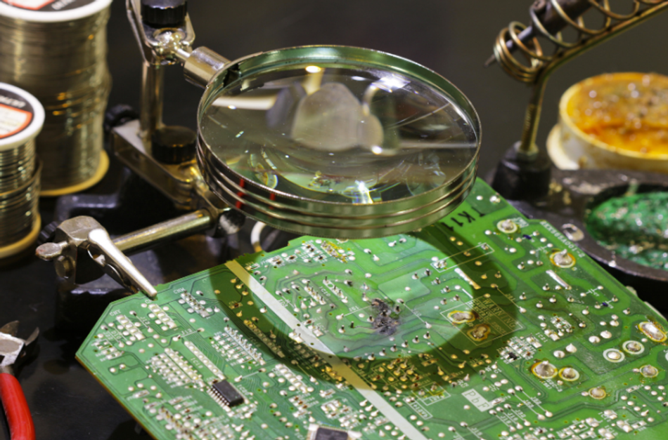
Visual Inspection
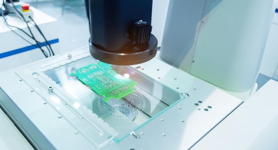
Visual inspection is a critical step in the quality control process for surface mount soldering. It involves examining solder joints and components on circuit boards for defects or irregularities that could compromise the performance and reliability of the assembled electronic devices. Visual inspection can be performed manually or with the help of automated optical inspection (AOI) systems.
Manual Visual Inspection: Manual visual inspection involves human operators closely examining PCBs under magnification to identify potential defects. This method allows human judgment in determining whether a solder joint is acceptable or requires rework. However, a manual inspection can be time-consuming and subject to human error. Tutorials show that skilled operators must ensure consistent and accurate inspection results.
Automated Optical Inspection (AOI): AOI systems use cameras, lighting, and image processing software to inspect PCBs for defects automatically. The AOI system compares the captured images with predefined criteria to identify anomalies. AOI offers several advantages over manual inspection, including increased speed, accuracy, and repeatability. AOI systems can detect many defects, including solder bridges, misaligned components, and insufficient solder.
Defect Detection: Visual inspection, whether manual or automated, aims to identify various types of soldering defects, such as:
Solder bridges: Unintended connections between solder joints can cause short circuits.
Insufficient solder: Inadequate solder volume on a joint, leading to weak mechanical and electrical connections.
Excessive solder: Too much solder on a joint, possibly causing short circuits or affecting the performance of nearby components.
Component misalignment: Incorrectly placed components can result in poor electrical connections or mechanical stress on the solder joints.
Post-Inspection Actions: After visual inspection, any detected defects must be addressed. Rework processes may be necessary to correct the identified issues, such as desoldering and resoldering components or removing excess solder. Documenting the inspection results and any rework actions is essential to maintain traceability and improve process control.
In conclusion, visual inspection is vital in ensuring the quality and reliability of surface mount soldering. By employing manual or automated techniques, manufacturers can detect and address soldering defects, enhancing the performance and longevity of their electronic products.
X-ray Inspection
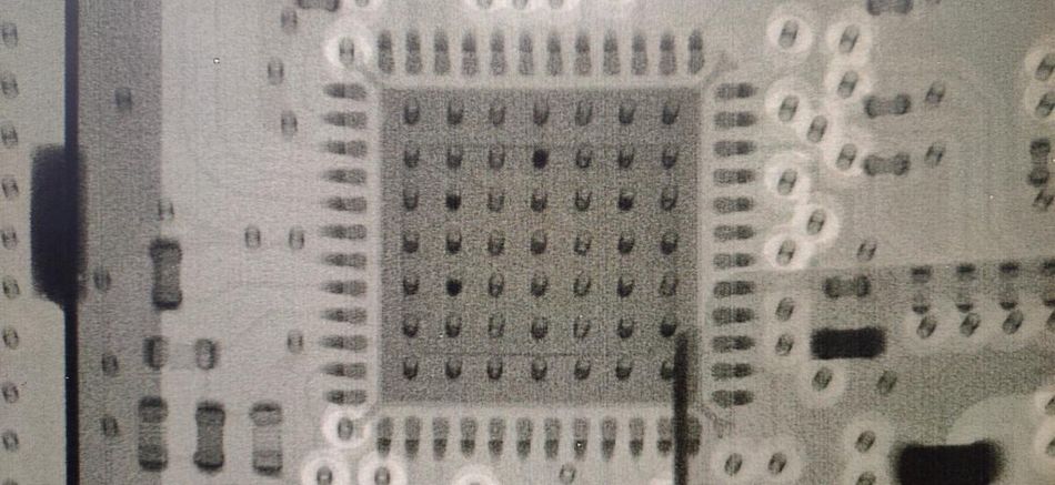
X-ray inspection is a non-destructive testing method used to evaluate the quality of solder joints and detect hidden defects in surface mount soldering. This technique is particularly useful for inspecting solder joints under components with limited or no optical accessibility, such as ball grid array (BGA) and quad flat no-lead (QFN) packages.
X-ray Inspection Process: X-ray inspection systems generate X-rays that pass through the PCB and are captured by a detector, creating a radiographic image of the internal structure of the solder joints. The contrast in the image is determined by the difference in the absorption of X-rays by the materials present, with denser materials, like metals, appearing brighter. Operators or automated image processing software analyze these images to identify potential defects.
Defect Detection: X-ray inspection is particularly effective in detecting defects that are difficult or impossible to identify using visual inspection methods. Some of these defects include:
Voiding: Air pockets or gaps within solder joints that can compromise the mechanical and thermal performance of the joint. X-ray inspection can reveal voids' size, shape, and location, allowing manufacturers to evaluate their impact on joint integrity.
Bridging: X-ray inspection can identify solder bridges beneath surface-mounted components where visual inspection is not feasible.
Insufficient or excessive solder: X-ray images can reveal the solder volume in hidden joints, helping identify cases of insufficient or excessive wave soldering that may affect joint performance.
X-ray Inspection Limitations: While X-ray inspection is a powerful tool, it has some limitations:
False Positives and Negatives: X-ray images may be subject to misinterpretation, leading to false-positive or false-negative defect identification. Careful analysis and correlation with other inspection methods are necessary to minimize this risk.
Material Limitations: X-ray inspection may be less effective for materials with similar X-ray absorption properties, making it difficult to differentiate between them in the captured image.
Complementary Inspection Techniques: X-ray inspection should be used with other inspection methods, such as visual and automated optical inspection, to ensure comprehensive defect detection and quality control. By combining multiple inspection techniques, manufacturers can more effectively identify and address potential issues, improving the reliability and performance of their products.
Automated Optical Inspection (AOI)
Automated Optical Inspection (AOI) is a non-contact, high-speed inspection method widely used in electronics manufacturing to ensure the quality of printed circuit board (PCB) assemblies. AOI systems employ cameras and image processing software to automatically inspect and compare PCBs against predefined criteria, identifying defects or deviations from the reference design.
AOI System Components: AOI systems typically consist of several key components:
High-resolution cameras: AOI systems use one or multiple cameras to capture detailed images of the PCB surface. Depending on the system configuration, cameras can be positioned at different angles to inspect the board from various perspectives, increasing the likelihood of detecting defects.
Lighting: Uniform and stable lighting is crucial for accurate image capture. AOI systems often use multiple light sources with different wavelengths and angles to create the desired contrast and minimize shadows.
Image processing software: The software processes the captured images, comparing them to reference images or design data to identify potential defects. Advanced AOI systems employ machine learning algorithms to improve inspection accuracy and adapt to variations in component appearance and solder joint quality.
Defect Detection: AOI systems are capable of detecting a wide range of defects, including:
Component presence, orientation, and alignment: AOI systems can verify that all components are present on the PCB, correctly oriented, and accurately aligned with their respective pads.
Solder joint quality: By analyzing the shape, size, and color of solder joints, AOI systems can identify soldering defects such as insufficient or excessive solder, bridging, and poor wetting.
- Component polarity: AOI systems can verify that they are mounted in the correct orientation for components with specific polarity requirements preventing potential malfunctions or damage.
Inspection Speed and Accuracy: One of the main advantages of AOI systems is their speed, inspecting thousands of components per hour, significantly faster than manual inspection methods. The accuracy of AOI systems depends on factors such as camera resolution, lighting conditions, and image processing algorithms. Typical AOI systems can achieve 90% or higher defect detection rates, with false call rates below 10%.
Limitations of AOI: While AOI is a powerful inspection method, it has some limitations:
- Hidden solder joints: AOI systems cannot inspect solder joints beneath smd components without optical access, such as BGAs or QFNs. X-ray inspection is required to assess the quality of these hidden joints.
Varying component appearances: Variations in component appearance due to manufacturing tolerances or changes in component suppliers can challenge AOI systems, potentially leading to false calls or missed defects. Regular system calibration and training can help mitigate this issue.
Integration with Other Inspection Methods: AOI is an essential part of a comprehensive inspection strategy, complementing other methods such as visual, X-ray, and functional testing. Manufacturers can more effectively identify and address potential issues by incorporating multiple inspection techniques, enhancing their products' overall quality and reliability.
Conclusion
In the electronics manufacturing industry, the reflow soldering process is crucial in ensuring reliable, high-quality PCB assemblies. By understanding the principles of reflow soldering, manufacturers can optimize their processes for consistent, high-quality results. Addressing challenges such as tombstoning, voids, and solder balling requires a thorough understanding of their root causes and the implementation of appropriate countermeasures. Inspection and quality control techniques are essential for verifying the quality of solder joints and identifying potential issues before they affect the final product's performance. By integrating these concepts and methods, manufacturers can achieve improved efficiency, yield, and product reliability in their electronics manufacturing processes.
FAQs
Q: What are the main phases of the reflow soldering process?
A: The reflow soldering process consists of four main phases: preheating, soaking, reflow, and cooling. Each phase serves a specific purpose, and carefully controlling the temperature profile is essential for achieving consistent, high-quality solder joints.
Q: What is the purpose of solder paste in reflow soldering?
A: Solder paste is a mixture of solder powder and flux, the bonding agent for attaching electronic components to PCBs during reflow soldering. The paste melts and wets the component leads and pads, forming a reliable electrical and mechanical connection.
Q: What are some common reflow soldering defects and their causes?
A: Common reflow soldering defects include tombstoning, voids, and solder balling. Tombstoning occurs when a component is lifted from the PCB due to uneven solder wetting. Voids are air pockets trapped inside solder joints, often caused by excessive outgassing or insufficient solder paste volume. Solder balling is the formation of small, unintended solder balls, which can be caused by improper reflow temperature profile or excessive solder paste.
Q: How can I ensure the quality of solder joints in my PCB assembly (PCBA)?
A: Implementing a comprehensive inspection strategy that includes visual, X-ray, and Automated Optical Inspection (AOI) can help identify potential issues and ensure the quality of solder joints. Manufacturers can address potential problems more effectively by incorporating multiple inspection techniques and enhancing their product quality and reliability.
Q: What is the importance of temperature profiling in reflow soldering?
A: Temperature profiling is critical for controlling the reflow soldering methods, as it directly impacts the quality of solder joints. A well-designed temperature profile ensures proper activation of flux, adequate wetting of component leads and pads, and controlled cooling, minimizing the risk of defects and ensuring reliable, high-quality solder joints.
References
1. Ning-Cheng Lee. Reflow Soldering Processes and Troubleshooting: SMT, BGA, CSP, and Flip Chip Technologies. [Cited 2023 May 24] Available from: Link
2. Wevolver. What is a stencil in PCB, and why do you need it?. [Cited 2023 May 24]
3. ScienceDirect. Thermal parameters optimization of a reflow soldering profile in printed circuit board assembly: A comparative study. [Cited 2023 May 24] Available from: Link
4. ScienceDirect. SMD Reflow Soldering: A Thermal Process Model. [Cited 2023 May 24] Available from: Link