Dry Etching vs Wet Etching: A Comprehensive Comparison
The semiconductor manufacturing field employs a range of etching techniques to craft intricate patterns and structures on material surfaces, with dry etching and wet etching being primary methods.

Last updated on 11 Oct, 2023. 21 minutes read
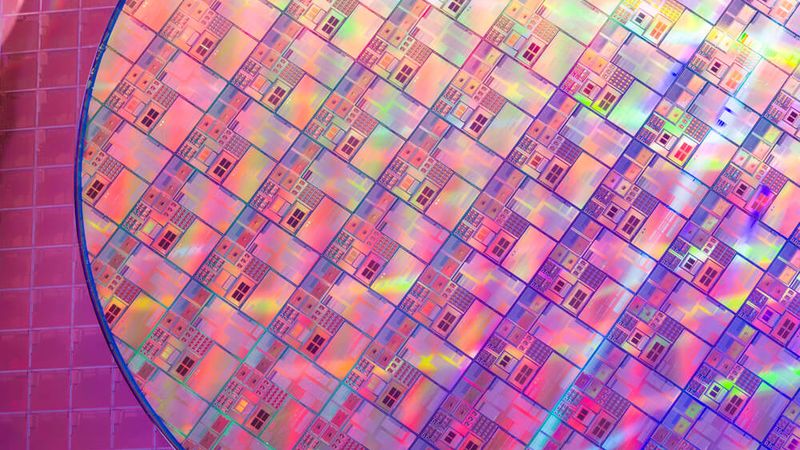
Thin Silicon Wafer
Introduction
Etching in semiconductor manufacturing refers to the selective removal of specific layers or patterns of materials from a semiconductor wafer's surface. This precise and controlled removal of materials is a fundamental step in creating the intricate structures and patterns necessary for the functioning of semiconductor devices. Etching defines various components on the semiconductor wafer, such as transistors, interconnects, and other elements that make up integrated circuits (ICs). Etching is also a critical process in microelectronic manufacturing, essential for creating functioning microelectromechanical systems (MEMS) and other components.
Etching plays a crucial role in the production of microelectronic components, with every substrate undergoing this essential process before reaching completion. Within the etching process, a protective masking material is applied to the substrate, rendering it resistant to the etching reagent's effects. This masking material can take various forms, including photoresists generated through lithography, or in certain instances, more durable masks like silicon nitride may be employed.
Etching processes are often classified based on the reagent phase used, with liquid and plasma or gaseous phases being the most common. When choosing an etching method, two critical factors come into play:
Isotropy and Anisotropy:
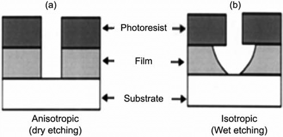
Isotropic etching maintains a constant etching rate in all directions, making material properties direction-independent.
In contrast, anisotropic etching selectively removes material along specific directions, introducing direction-dependent properties.
Selectivity:
Selectivity refers to the relative etch rates between a masking material (used for patterning) and the material of interest.
While liquid and gas chemical etches typically offer high selectivity, they tend to be isotropic, posing challenges in controlling etch rates.
Plasma etching provides a degree of control and can be tailored to be highly anisotropic, though achieving excellent selectivity can be more demanding.
There are two primary methods of etching used in semiconductor fabrication. Read on to learn more.
Dry Etching
Definition and Basic Principles
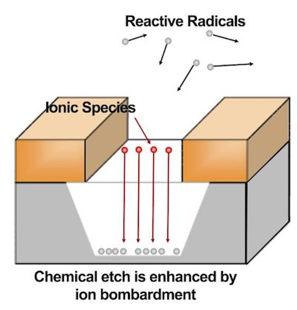
Dry etching, a pivotal material removal technique, harnesses the potency of plasma—a highly reactive and energetic gas—for selective material removal from a substrate. Plasma generation is initiated by applying an electric field to a low-pressure gas, leading to the ionization of gas molecules and the creation of a blend of ions, electrons, and neutral species. These reactive entities then engage with the substrate surface, orchestrating material removal through a synergy of chemical reactions and physical sputtering.
The core tenets of dry etching revolve around the meticulous control of plasma generation, ion acceleration, and chemical reactions to attain desired etching outcomes. Plasma generation is typically facilitated via radio frequency (RF) or microwave power sources, which furnish the requisite energy for gas molecule ionization. Ion acceleration, on the other hand, is regulated through the application of a bias voltage to the substrate, compelling positively charged ions toward the surface. The intricate chemistry between the reactive species and the substrate material hinges on the selection of etching gas, gas pressure, and process temperature.
Dry etching can be used to etch a wide range of materials, including metals, semiconductors, dielectrics, and polymers. The choice of etching gas and process parameters can be tailored to achieve high selectivity, meaning that the etching process preferentially removes one material over another. This is particularly important in semiconductor manufacturing, where multiple layers of different materials are often patterned on a single substrate.
Exploring Diverse Varieties of Dry Etching
In the broader context, dry etching spans a spectrum of diverse technologies, including but not limited to
Reactive Ion Etching (RIE)
Reactive Ion Etching (RIE) is a widely used dry etching technique that combines both chemical and physical processes to remove material from a substrate. In RIE, plasma is generated by applying radio frequency (RF) power to a low-pressure gas mixture, typically containing a reactive gas such as CF4, SF6, or Cl2, and an inert gas like argon. The reactive gas molecules are ionized and dissociated in the plasma, forming highly reactive species that can react with the substrate material. At the same time, the ions are accelerated towards the substrate by an electric field, causing physical sputtering of the material.
The advantages of RIE include its ability to achieve high etching rates, good selectivity, and anisotropic etching profiles. Anisotropic etching refers to the preferential removal of material in one direction, resulting in vertical sidewalls and well-defined features. This is particularly important in semiconductor manufacturing, where precise control over feature dimensions is critical for device performance.
However, RIE also has some disadvantages, such as the potential for damage to the substrate due to the high-energy ion bombardment. This can lead to defects, such as lattice damage or amorphous layer formation, which can negatively impact device performance. Additionally, RIE can suffer from non-uniform etching across the substrate, especially when the etching rate is sensitive to variations in process parameters or plasma distribution.
RIE is widely used in semiconductor manufacturing for a variety of applications, including the etching of silicon, silicon dioxide, silicon nitride, and metal layers. It is also employed in the fabrication of microelectromechanical systems (MEMS), where precise control over feature dimensions and aspect ratios is essential for device functionality.
Deep Reactive Ion Etching (DRIE)
Deep Reactive Ion Etching (DRIE) is a specialized dry etching technique designed to create high-aspect-ratio structures, such as deep trenches and through-silicon vias, in silicon substrates. DRIE builds upon the principles of Reactive Ion Etching (RIE) but employs a unique process known as the Bosch process, which alternates between two distinct etching and passivation steps to achieve deep, anisotropic etching profiles.
In the etching step, a plasma containing reactive species, such as SF6, is used to chemically etch the silicon substrate. The ions in the plasma are accelerated towards the substrate, removing material through a combination of chemical reactions and physical sputtering. Following the etching step, a passivation step is performed using a different gas, typically C4F8, which forms a protective polymer layer on the sidewalls of the etched features. This passivation layer protects the sidewalls from further etching during subsequent cycles, resulting in highly anisotropic etching profiles with nearly vertical sidewalls.
The advantages of DRIE include its ability to achieve high-aspect-ratio structures with depths up to several hundred micrometers while maintaining excellent sidewall smoothness and uniformity. This makes DRIE particularly well-suited for applications in microelectromechanical systems (MEMS) fabrication, where deep trenches, through-silicon vias, and other high-aspect-ratio structures are often required.
However, DRIE also has some challenges, such as the formation of scalloping or roughness on the sidewalls due to the cyclic nature of the Bosch process. Additionally, DRIE can be more complex and time-consuming compared to conventional RIE, as it requires precise control over the etching and passivation steps to achieve the desired etching profiles.
Despite these challenges, DRIE has become an essential tool in MEMS fabrication and other applications requiring high-aspect-ratio structures in silicon substrates. Its ability to create deep, well-defined features with minimal damage to the substrate makes it a valuable technique in the field of semiconductor manufacturing.
Sputter Etching/Ion Milling
Sputter etching, also known as ion milling, is a vacuum-based process conducted at low pressures, typically around 10 millipascals (mPa). In this technique, argon gas is commonly employed. The process harnesses the kinetic energy of gas molecules to displace unwanted material layers from the substrate's surface. Sputter etching primarily relies on physical mechanisms to achieve precise material removal, making it a valuable technique in various applications.
Further reading: Ion Milling: A Comprehensive Guide to Material Etching Techniques
Equipment and Process Parameters
Dry etching processes require specialized equipment to generate and control the plasma, as well as to maintain the necessary process conditions for optimal etching performance. The primary components of a dry etching system include a vacuum chamber, a gas delivery system, an RF or microwave power source, and a substrate holder or chuck. The vacuum chamber is designed to maintain a low-pressure environment, typically in the range of a few millitorr to several tens of millitorr, which is necessary for plasma generation and stable etching conditions.
The gas delivery system introduces the etching gas mixture into the chamber, while the power source provides the energy needed to ionize the gas molecules and create the plasma. The substrate holder or chuck is used to secure the substrate in the chamber and can be biased with an electric potential to control the ion acceleration towards the surface.
Key process parameters that influence dry etching performance include gas pressure, gas flow rate, power source settings, and substrate bias voltage. Gas pressure affects the density and reactivity of the plasma, with lower pressures generally leading to higher ionization rates and more reactive species. The gas flow rate determines the availability of reactive species at the substrate surface and can influence the etching rate and uniformity. Power source settings, such as RF power and frequency, control the energy input to the plasma and can impact the ionization efficiency and plasma stability. Substrate bias voltage affects the acceleration of ions toward the surface, which in turn influences the etching rate, selectivity, and profile control.
Controlling these process parameters is crucial for achieving the desired etching characteristics and ensuring consistent results across the substrate. However, this can be challenging due to the complex interactions between the plasma, reactive species, and substrate material, as well as the potential for process drift and non-uniformities in the plasma distribution. Advanced process control techniques, such as in-situ monitoring and feedback control, are often employed to maintain stable and reproducible etching conditions.
Wet Etching
Definition and Basic Principles
Wet etching is a chemical process that involves the selective removal of material from a substrate using liquid etchants. These etchants are typically composed of a mixture of chemicals, such as acids, bases, or solvents, which react with the substrate material to form soluble products that can be easily washed away. The etching process is driven by chemical reactions at the substrate-etchant interface, with the etching rate determined by the reaction kinetics and the concentration of the reactive species in the solution.
The basic principles of wet etching involve controlling the etchant composition, concentration, and temperature to achieve the desired etching characteristics. The etchant composition determines the reactivity of the solution and the types of materials that can be etched, while the concentration of the reactive species influences the etching rate and selectivity. The temperature of the etchant affects the reaction kinetics, with higher temperatures generally leading to faster etching rates and increased chemical activity.
Wet etching can be used to etch a wide range of materials, including metals, semiconductors, dielectrics, and polymers. The choice of etchant and process parameters can be tailored to achieve high selectivity, meaning that the etching process preferentially removes one material over another. This is particularly important in semiconductor manufacturing, where multiple layers of different materials are often patterned on a single substrate.
Exploring the Diverse Types of Wet Etching
Wet etching, a fundamental process in microfabrication, encompasses various types, each tailored for specific applications. Here are some common types of wet etching:
Isotropic Etching
Isotropic etching is a type of wet etching process in which the material removal occurs uniformly in all directions. This results in etched features with rounded or tapered profiles, as the etchant attacks the substrate material at the same rate, regardless of the crystallographic orientation or the geometry of the features. Isotropic etching is primarily driven by chemical reactions between the etchant and the substrate material, with minimal influence from physical processes such as diffusion or mass transport.
The primary advantage of isotropic etching is its simplicity and ease of implementation, as it typically requires only a single etchant solution and minimal process control. This makes it suitable for applications where precise control over feature dimensions is not critical, such as bulk material removal or rough surface preparation. However, isotropic etching can be less desirable for applications requiring well-defined features with vertical sidewalls, as the etching process tends to undercut the mask and create rounded profiles.
Isotropic etching is widely used in semiconductor manufacturing for a variety of applications, including the removal of sacrificial layers, surface cleaning, and the etching of non-critical features. Common etchants used for isotropic etching include hydrofluoric acid (HF) for silicon dioxide, potassium hydroxide (KOH) for silicon and phosphoric acid for aluminum. The choice of etchant and process parameters can be tailored to achieve the desired etching rate, selectivity, and profile control, depending on the specific application requirements.
Anisotropic Etching
Anisotropic etching is a type of wet etching process that results in the preferential removal of material in a specific direction, leading to etched features with well-defined, vertical sidewalls. Unlike isotropic etching, which occurs uniformly in all directions, anisotropic etching relies on the crystallographic orientation of the substrate material and the selective reactivity of the etchant to achieve directional etching profiles.
The primary advantage of anisotropic etching is its ability to create well-defined features with minimal undercutting of the mask, making it suitable for applications requiring precise control over feature dimensions and aspect ratios. This is particularly important in semiconductor manufacturing, where the performance of devices often depends on the accuracy and uniformity of the etched features.
However, anisotropic etching can be more complex and challenging to implement compared to isotropic etching, as it requires a thorough understanding of the substrate material's crystallographic properties and the etchant's reactivity. Additionally, anisotropic etching may be sensitive to variations in process parameters, such as etchant concentration, temperature, and agitation, which can impact the etching rate and profile control.
Anisotropic etching is widely used in semiconductor manufacturing for a variety of applications, including the fabrication of high-aspect-ratio structures, such as trenches, vias, and channels. Common etchants used for anisotropic etching include tetramethylammonium hydroxide (TMAH) for silicon and buffered oxide etchants (BOE) for silicon dioxide. The choice of etchant and process parameters can be tailored to achieve the desired etching rate, selectivity, and profile control, depending on the specific application requirements.
However, it is also important to know that some processes combine both isotropic and anisotropic characteristics, offering a balance between uniformity and directional control. This is often referred to as Isotropic/Anisotropic Wet Etching.
Equipment and Process Parameters
Wet etching processes typically require relatively simple equipment compared to dry etching techniques. The primary components of a wet etching system include a chemical-resistant container or bath, a temperature control system, and a means of agitation or stirring. The container or bath is used to hold the etchant solution, while the temperature control system maintains the desired process temperature, which can significantly impact the etching rate and selectivity. Agitation or stirring is often employed to ensure uniform etching across the substrate by promoting the transport of reactive species to the substrate surface and the removal of reaction products.
Key process parameters that influence wet etching performance include etchant composition, concentration, temperature, and process time. The etchant composition determines the reactivity of the solution and the types of materials that can be etched, while the concentration of the reactive species influences the etching rate and selectivity. The temperature of the etchant affects the reaction kinetics, with higher temperatures generally leading to faster etching rates and increased chemical activity. Process time determines the duration of the etching process and directly impacts the depth of the etched features.
Controlling these process parameters is essential for achieving the desired etching characteristics and ensuring consistent results across the substrate. However, this can be challenging due to the complex interactions between the etchant, substrate material, and process conditions. In addition, wet etching processes can be sensitive to variations in etchant composition, concentration, and temperature, which can lead to non-uniform etching and reduced process repeatability. To address these challenges, advanced process control techniques, such as in-line monitoring and feedback control, can be employed to maintain stable and reproducible etching conditions.
 Isotropic and Anisotropic - Image credits: Characterization of low-pressure plasma-dc glow discharges (Ar, SF6, and SF6/He) for Si etching
Comparison of Dry Etching and Wet Etching
Dry etching and wet etching are two prominent techniques in semiconductor manufacturing, each with its advantages and drawbacks. By understanding the distinctions between dry and wet etching, manufacturers can make informed decisions about which technique to use for specific applications, contributing to the development of cutting-edge microelectronic devices and integrated circuits. In this section, we’ll highlight the differences between these two processes:
Etching Rate
The etching rate, defined as the amount of material removed per unit of time, is a critical parameter in both dry and wet etching processes. It directly impacts the process throughput, feature dimensions, and overall process efficiency. Comparing the etching rates of dry and wet etching techniques reveals some key differences and trade-offs between the two methods.
Dry etching processes, such as Reactive Ion Etching (RIE), generally exhibit higher etching rates compared to wet etching techniques. This is due to the combined effects of chemical reactions and physical sputtering, which can lead to more efficient material removal. Additionally, dry etching processes can be tailored to achieve high etching rates for specific materials by adjusting the plasma parameters, such as gas composition, pressure, and power settings.
On the other hand, wet etching rates are primarily determined by the chemical reactivity of the etchant and the substrate material, as well as the etchant concentration and temperature. While wet etching can achieve high etching rates for certain materials and etchant combinations, it is generally less versatile and adaptable compared to dry etching techniques.
The choice between dry and wet etching based on the etching rate depends on the specific application requirements, such as the desired feature dimensions, process throughput, and material compatibility. In some cases, a combination of both techniques may be employed to achieve the optimal balance between etching rate, selectivity, and profile control.
Selectivity
Selectivity is a critical parameter in etching processes, as it determines the ability of the etching technique to preferentially remove one material over another. High selectivity is essential in semiconductor manufacturing and microfabrication, where multiple layers of different materials are often patterned on a single substrate. Comparing the selectivity of dry and wet etching techniques reveals some key differences and trade-offs between the two methods.
In dry etching processes, such as Reactive Ion Etching (RIE), selectivity can be achieved by carefully controlling the plasma parameters, such as gas composition, pressure, and power settings. By selecting the appropriate etching gas and process conditions, it is possible to achieve high selectivity for specific material combinations. For example, fluorine-based plasmas can be used to selectively etch silicon dioxide over silicon, while chlorine-based plasmas can be used to selectively etch metals such as aluminum or copper. However, achieving high selectivity in dry etching processes can be challenging due to the complex interactions between the plasma, reactive species, and substrate material, as well as the potential for process drift and non-uniformities in the plasma distribution.
Wet etching techniques, on the other hand, rely on the selective reactivity of the etchant and the substrate material to achieve high selectivity. By choosing an etchant that preferentially reacts with one material over another, it is possible to achieve high selectivity with relatively simple process control. For example, hydrofluoric acid (HF) can be used to selectively etch silicon dioxide over silicon, while phosphoric acid can be used to selectively etch aluminum over silicon dioxide. However, wet etching selectivity can be limited by the availability of suitable etchants for specific material combinations and the potential for side reactions or etchant depletion, which can reduce the overall process efficiency.
The choice between dry and wet etching based on selectivity depends on the specific application requirements, such as the desired feature dimensions, material compatibility, and process complexity. In some cases, a combination of both techniques may be employed to achieve the optimal balance between selectivity, etching rate, and profile control.
Profile Control and Surface Quality
Profile control and surface quality are important factors to consider when comparing dry and wet etching techniques, as they directly impact the functionality and performance of the fabricated devices. Profile control refers to the ability of the etching process to create well-defined features with the desired shape and dimensions, while surface quality refers to the smoothness and defect-free nature of the etched surfaces.
Dry etching processes, such as Reactive Ion Etching (RIE), generally offer better profile control compared to wet etching techniques. This is due to the anisotropic nature of dry etching, which results in the preferential removal of material in one direction, leading to vertical sidewalls and well-defined features. Additionally, dry etching processes can be tailored to achieve specific etching profiles by adjusting the plasma parameters, such as gas composition, pressure, and power settings. However, dry etching can sometimes result in surface damage due to the high-energy ion bombardment, which can lead to defects, such as lattice damage or amorphous layer formation, that can negatively impact device performance.
Wet etching techniques, on the other hand, can achieve high surface quality due to the chemical nature of the etching process, which typically results in smoother and more defect-free surfaces compared to dry etching. However, wet etching processes generally offer less profile control, as they are more prone to isotropic etching, which can lead to rounded or tapered profiles and undercutting of the mask. In some cases, anisotropic wet etching can be achieved using etchants that selectively react with specific crystallographic planes of the substrate material, but this is highly dependent on the substrate orientation and etchant composition.
The choice between dry and wet etching based on profile control and surface quality depends on the specific application requirements, such as the desired feature dimensions, material compatibility, and process complexity. In some cases, a combination of both techniques may be employed to achieve the optimal balance between profile control, surface quality, and other process parameters, such as etching rate and selectivity.
Further reading: Comprehensive Guide to Surface Profile: Techniques, Applications, and Importance
Environmental and Safety Considerations
Environmental and safety considerations play a significant role in the choice between dry and wet etching techniques, as they can impact the overall sustainability, cost, and regulatory compliance of the manufacturing process.
Dry etching processes, such as Reactive Ion Etching (RIE), typically involve the use of hazardous gases, such as fluorine or chlorine-based compounds, which can pose risks to human health and the environment if not properly managed. Additionally, the generation of plasma in dry etching processes can produce toxic byproducts and greenhouse gases, such as perfluorocarbons (PFCs), which contribute to global warming. To mitigate these risks, dry etching systems must be equipped with proper gas handling, abatement, and exhaust systems to ensure the safe disposal of hazardous gases and byproducts. These safety measures can add complexity and cost to the dry etching process, as well as increase the overall environmental footprint of the manufacturing facility.
Wet etching techniques, on the other hand, involve the use of liquid etchants, which can also pose environmental and safety risks if not properly managed. Many etchants used in wet etching processes, such as hydrofluoric acid (HF) or potassium hydroxide (KOH), are highly corrosive and toxic, requiring careful handling, storage, and disposal to prevent harm to workers and the environment. Additionally, the large volumes of spent etchant and rinse water generated during wet etching processes can result in significant waste disposal challenges, as these waste streams often contain hazardous chemicals and heavy metals that must be treated before disposal. However, wet etching processes generally have a lower environmental impact compared to dry etching, as they do not produce greenhouse gases or require energy-intensive plasma generation.
The choice between dry and wet etching based on environmental and safety considerations depends on the specific application requirements, as well as the availability of resources and infrastructure for managing hazardous materials and waste streams. In some cases, a combination of both techniques may be employed to achieve the optimal balance between process performance, environmental impact, and safety compliance.
Unlocking the Versatility of Etching: Applications You Should Explore
Across the realms of electronics, printing industries, and precision machinery, electrolytic and chemical etching have stood as foundational technologies. Although modern advancements have sidelined etching in some spheres, its role as a versatile processing tool remains paramount. Here, we delve into some notable etching applications that continue to shape various industries.
PCB Etching: The Unseen Force in Circuitry
In the ever-evolving world of printed circuit boards (PCBs), where the demand for precision knows no bounds, PCB etching emerges as an unsung hero. As impedance requirements for wires reach new heights, necessitating precise wire width control, the PCB industry witnesses remarkable growth and innovation. The quality and reliability of PCBs have soared in industrial manufacturing, ushering in an era of diversified and exemplary design processes.
PCB etching, a pivotal procedure in PCB manufacturing, takes center stage. This process involves the meticulous removal of excess copper, and unveiling pristine circuit layouts. It encompasses the removal of unwanted copper (Cu) from the board post-PCB design, sculpting the desired circuit pattern. The base copper, often referred to as start copper, gracefully yields to the etching process. In comparison to electroplated copper, rolled and heat-treated copper proves more amenable to etching.
Before embarking on the etching journey, a meticulously crafted layout blueprint ensures that the final product aligns seamlessly with the designer's vision. Photolithography, a precise technique, transfers the designer's circuit image onto the PCB, serving as the blueprint for copper removal. Distinct etching techniques distinguish inner and exterior layer etching processes. Outer layer etching employs tin plating as the etch resist, safeguarding designated circuitry. Conversely, the inner layer relies on the photoresist as the etched resistor.
In PCB etching, virtually all copper surrenders to the process, except circuitry shielded by prior tin plating. After the meticulous removal of tin and comprehensive copper cleaning, the circuit is primed to advance to subsequent production stages.
Semiconductor Etching: Precision Redefined in Microelectronics
Semiconductor etching stands as a linchpin in the realm of microelectronics, playing a transformative role in enhancing the performance and attributes of semiconducting materials pivotal to electronic device production. This intricate process shapes surface features that optimize electrical device functionality. Notably, plasma etching emerges as a stalwart technique.
Plasma etching finds its niche in crafting deep trenches on silicon surfaces, a boon for Micro-Electro-Mechanical Systems (MEMS) applications. As microelectronics continue to advance, the role of plasma etching is poised to expand, potentially extending its influence to the nanoscale.
Hydrogen plasma etching, in particular, piques scientific interest with its myriad applications. This method shines in removing sections of native oxides from semiconductor surfaces during the etching process. Additionally, it yields a chemically pristine and balanced surface, catering to a diverse array of applications and offering tantalizing possibilities in the semiconductor industry.
Choosing the Right Etching Technique
Selecting the appropriate etching technique for a specific application requires a thorough understanding of the material properties, desired feature dimensions, and process requirements. The following guidelines can help in making an informed decision when choosing between dry and wet etching techniques:
Material compatibility: Consider the types of materials that need to be etched and the availability of suitable etchants or plasma chemistries for each technique. Some materials may be more effectively etched using dry etching processes, while others may be more suitable for wet etching.
Feature dimensions and profile control: Evaluate the desired feature dimensions, aspect ratios, and profile control requirements for the application. Dry etching techniques, such as Reactive Ion Etching (RIE), generally offer better profile control and anisotropic etching profiles, making them more suitable for applications requiring well-defined features with vertical sidewalls.
Etching rate and selectivity: Assess the etching rate and selectivity requirements for the application. Dry etching processes typically exhibit higher etching rates and can be tailored to achieve high selectivity for specific material combinations. However, wet etching techniques may offer simpler process control and lower environmental impact, depending on the specific etchant and process conditions.
Environmental and safety considerations: Evaluate the environmental and safety implications of each technique, including the management of hazardous materials, waste disposal, and greenhouse gas emissions. Wet etching processes generally have a lower environmental impact compared to dry etching but may require more extensive waste treatment and disposal infrastructure.
Cost and equipment complexity: Consider the cost and complexity of the equipment and process control required for each technique. Dry etching processes typically involve more complex equipment and process control, which can increase the overall cost and maintenance requirements. Wet etching techniques, on the other hand, generally require simpler equipment and process control, making them more cost-effective for certain applications.
By carefully considering these factors and weighing the trade-offs between dry and wet etching techniques, it is possible to select the most appropriate etching method for a specific application. In some cases, a combination of both techniques may be employed to achieve the optimal balance between process performance, environmental impact, and cost.
Conclusion
Understanding the differences between dry etching and wet etching techniques is crucial for selecting the appropriate method for specific applications in semiconductor manufacturing and microfabrication. Dry etching processes, such as Reactive Ion Etching (RIE), offer better profile control, higher etching rates, and greater versatility in terms of material compatibility. However, they can be more complex, costly, and have a higher environmental impact compared to wet etching techniques. Wet etching processes, on the other hand, generally provide simpler process control, lower cost, and better surface quality but may offer less profile control and selectivity. By carefully considering the material properties, desired feature dimensions, process requirements, environmental impact, and cost, it is possible to choose the most appropriate etching technique for a specific application.
Frequently Asked Questions (FAQs)
What is the main difference between dry etching and wet etching? Dry etching uses plasma to remove material from a substrate, while wet etching relies on chemical reactions in liquid solutions.
Which etching technique is better for creating well-defined features with vertical sidewalls? Dry etching techniques, such as Reactive Ion Etching (RIE), generally offer better profile control and anisotropic etching profiles, making them more suitable for applications requiring well-defined features with vertical sidewalls.
Can both dry and wet etching techniques be used for the same material? Yes, both dry and wet etching techniques can be used for the same material, but the choice of technique depends on the specific application requirements, such as desired feature dimensions, process throughput, and material compatibility.
Which etching technique has a lower environmental impact? Wet etching processes generally have a lower environmental impact compared to dry etching, as they do not produce greenhouse gases or require energy-intensive plasma generation. However, wet etching processes can generate large volumes of hazardous waste that must be treated before disposal.
How can I choose the right etching technique for my application? Consider factors such as material compatibility, desired feature dimensions, process requirements, environmental impact, and cost when choosing between dry and wet etching techniques. In some cases, a combination of both techniques may be employed to achieve the optimal balance between process performance, environmental impact, and cost.
Reference
ByJu's Classes (2021). Difference between Isotropic and Anisotropic. Available at: https://byjus.com/chemistry/difference-between-isotropic-and-anisotropic/ [Accessed 2nd December, 2021]
Etch Overview for Microsystems (n.a) Southwest Centers for Microsystems Education. Available at: https://www.google.com/url?sa=t&source=web&rct=j&url=https://nanoscale.unl.edu/pdf/Etching_Overview_LM_PG.pdf&ved=2ahUKEwja6-O3us30AhVI6qQKHSMcAPsQFnoECC4QAQ&usg=AOvVaw2ZhDgFeyqTKPvFBZaX9rIc [Accessed 1st December, 2021]
MEMS and Nanotechnology Exchange (2020). Available at: https://www.mems-exchange.org/MEMS/processes/etch.html [Accessed 1st December, 2021]
Kiihamäki J, Kattelus H, Karttunen J, Franssila S (2000) Depth and profile control in plasma etched MEMS structures. Sens Actuators 82:234–238 Google Scholar
Bosch Today (2018). Bosch Global. [Accessed 1st December, 2021]
Yeom, J., et.al(2005). Journal of Vacuum Science & Technology B Microelectronics and Nanometer Structures. DOI: 10.1116/1.2101678
Jaeger, Richard C. (2002). "Lithography". Introduction to Microelectronic Fabrication (2nd ed.). Upper Saddle River: Prentice Hall. ISBN 978-0-201-44494-0.
Gad-el-Hak M (2002) The MEMS Handbook. CRC Press LLC, Boca Raton. Available at: https://scholar.google.com/scholar_lookup?title=The%20MEMS%20Handbook&publication_year=2002&author=Gad-el-Hak%2CM [Accessed 2nd December, 2021]
Gong, L.(2016) PCB Etching Technique and Analysis Solution. Available at: https://www.seeedstudio.com/blog/2017/03/16/pcb-etching/ [Accessed 3rd December, 2021]
in this article
1. Introduction2. Dry Etching3. Wet Etching4. Isotropic and Anisotropic - Image credits: Characterization of low-pressure plasma-dc glow discharges (Ar, SF6, and SF6/He) for Si etching5. Comparison of Dry Etching and Wet Etching6. Unlocking the Versatility of Etching: Applications You Should Explore7. Choosing the Right Etching Technique8. Conclusion9. Frequently Asked Questions (FAQs)10. Reference