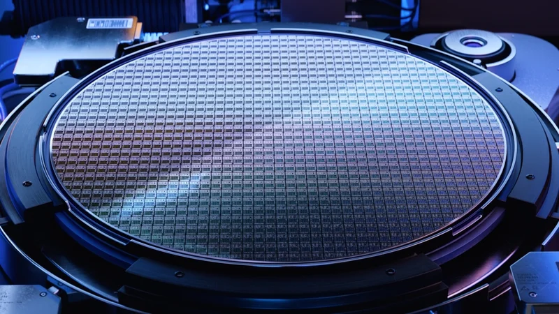
200 mm Wafer vs 300 mm Wafer – A Technical Comparison for Engineers
A wafer is the thin substrate used to build integrated circuits in semiconductor manufacturing. This article compares 200mm and 300mm wafer sizes, covering die count, fabs, process nodes, costs, and applications in CPUs, GPUs, automotive, analog, IoT, and more.

09 Sep, 2025. 19 minutes read
Key Takeaways
Surface Area & Die Capacity
A 300 mm wafer provides more than twice the surface area of a 200 mm wafer, approximately 70,700 mm² vs. 31,400 mm², allowing for significantly more integrated circuits per wafer. This translates into improved manufacturing throughput and lower cost per chip.Manufacturing Efficiency & Cost Savings
Larger wafers enable better automation and reduce per-die costs due to the increased die density. However, ramping up to 300 mm requires substantial investment in new fabrication tools and infrastructure.Different Applications, Different Wafers
200 mm wafers remain critical for legacy and specialty markets, such as MEMS, RF chips, analog ICs, and power semiconductors, where advanced node scaling isn’t necessary.
300 mm wafers dominate advanced computing chips, like DRAM, NAND flash, and logic devices, especially at process nodes below 10 nm.
Economic Viability & Industry Trends
Transitioning to 300 mm wafers drives efficiency; even if the initial capital cost is high, the long-term savings on die production justify it for high-volume, advanced applications.
Despite this, many fabs continue expanding 200 mm capacity due to continued demand in critical but mature sectors. Recent data even shows faster shipment growth for 200 mm wafers than 300 mm in 2021, underlining their enduring importance.
Handling & Tooling Considerations
While 300 mm wafers carry more risk in terms of fragility and tooling complexity, they can move the same distance in manufacturing as 200 mm wafers, yet handle more area, increasing cost-efficiency in handling and processing.Scaling Beyond 300 mm: Challenges Ahead
The industry has explored 450 mm wafer technology, but uptake has stalled. Higher equipment and operational costs, along with limited cost-per-die gains (especially in lithography-dominated stages), have made this transition impractical for most manufacturers.
Introduction
In semiconductor manufacturing, wafer size defines both the economics and technical capabilities of integrated circuit production. A silicon wafer is a thin substrate where billions of transistors are patterned using advanced lithography. The diameter of the wafer directly impacts die count, yield behavior, thermal properties, and overall manufacturing costs.
The 200mm wafer (8-inch), introduced in high-volume fabs in the late 1990s, provided ~31,400 mm² of surface area and enabled process nodes from 90nm down to 28nm. These mature nodes remain optimal for analog, MEMS, automotive, and power devices where reliability and long product lifecycles are essential.
By contrast, the 300mm wafer (12-inch), which offers ~70,700 mm² of usable area—2.25× more than a 200mm wafer—became the foundation for cutting-edge logic and memory. A single 300mm wafer can produce more than 300 dies of 15 mm × 15 mm each, compared to ~139 on a 200mm wafer. This scaling reduces per-chip processing costs by ~40%, even though the capital cost of building a 300mm fab exceeds $20 billion, compared to <$2 billion for a 200mm fab.
Today, foundries such as Intel, TSMC, and Samsung rely on 300mm fabs to manufacture CPUs, GPUs, DRAM, and high-performance processors at sub-10nm nodes using EUV lithography. Meanwhile, 200mm fabs continue to expand for specialty technologies, driven by strong demand in automotive, IoT, and industrial sectors. Together, both wafer sizes remain essential pillars of the semiconductor industry and its supply chain.
Evolution of Wafer Sizes
Historical progression
The evolution of silicon wafers has closely followed the scaling demands of the semiconductor industry. Early devices in the 1960s were built on 25 mm wafers, each capable of holding only a few transistors. As wafer size increased to 100 mm (4-inch) in the 1980s, the available surface area expanded enough to support hundreds of integrated circuits per wafer. By the 1990s, the industry transitioned to 150 mm wafers, enabling smaller feature sizes below 1 µm and improving yield through better process control.
The introduction of the 200mm wafer in the late 1990s marked a major leap. With a wafer diameter of 200 mm (8-inch), the surface area nearly quadrupled compared to 150 mm wafers, allowing more dies per wafer and supporting process nodes down to 90 nm and 65 nm. These nodes were ideal for cost-effective semiconductor manufacturing of analog ICs, MEMS, and power devices.
Commercial production of 300mm wafers began in the early 2000s, providing 2.25× the surface area of a 200mm wafer. This increase in wafer diameter made it possible to manufacture chips containing billions of transistors, pushing process nodes to 10 nm and below. Larger wafer sizes reduced the cost per die, but also required advanced lithography, automation, and new fab infrastructure.
This steady growth in wafer size illustrates the fundamental trade-off in semiconductor manufacturing: each new generation of silicon wafers delivers greater transistor density and lower cost per chip, but at the expense of higher fab complexity and capital investment.
Recommended reading: Silicon Wafers: Production, Properties and Application
Surface Area and Die Count
The geometric advantage of larger wafer sizes is straightforward: surface area increases with the square of the wafer diameter. A 200mm wafer (8-inch) has a usable area of roughly 31,400 mm², while a 300mm wafer (12-inch) provides ~70,700 mm²—a 2.25× increase in available silicon.
This scaling directly affects dies per wafer. For example, with a standard 15 mm × 15 mm die size, a 200mm wafer yields about 139 functional dies, while a 300mm wafer produces more than 314 dies, even after accounting for edge losses. In practice, die count can vary depending on chip design, defect density, and scribe line overhead, but the proportional gain from a larger wafer is always significant.
The larger wafer diameter also allows manufacturers to fabricate bigger dies that are impractical on 200mm wafers. High-performance CPUs, GPUs, and AI processors often exceed 400 mm² per die, a scale that only 300mm fabs can support efficiently. Meanwhile, mature 200mm fabs focus on smaller die sizes for analog, MEMS, automotive, and IoT devices, where cost, reliability, and high-volume production are prioritized over extreme transistor density.
Ultimately, the relationship between wafer size and die count highlights the economic foundation of semiconductor manufacturing: more dies per wafer means lower cost per chip, provided yield remains controlled. This is why foundries invest heavily in 300mm fabs for cutting-edge logic, while 200mm fabs remain indispensable for specialty devices and mature nodes.
Geometric comparison of 200 mm and 300 mm wafers
The area of a circular wafer is determined by the equation A = π × (d/2)², where d is the wafer diameter. Increasing wafer diameter significantly increases usable surface area, which directly translates into higher dies per wafer.
| Parameter | 200mm Wafer | 300mm wafer | Explanation |
| Wafer diameter | 200 mm (8 in) | 300 mm (12 in | Standard wafer diameters in semiconductor fabrication |
| Surface area | ~31,416 mm² | ~70,685 mm² | 300mm wafers provide ~2.25× more area (π·r²) |
| Area ratio | 1 | 2.25 | Derived from (300/200)² = 9/4 |
| Typical 15 mm × 15 mm dies | ≈139 dies/wafer | ≈314 dies/wafer | Simplified calculation, ignoring edge losses and defects |
| Maximum die count (typical) | 100–125 dies | 229–450 dies | Actual yield depends on die size and defect density |
Because a 300mm wafer offers 2.25× the surface area of a 200mm wafer, it enables significantly higher die-per-wafer output, reinforcing its role in high-volume, cost-sensitive chip production.
Yield Considerations
Yield in semiconductor manufacturing refers to the fraction of dies per wafer that function correctly after fabrication. As wafer size increases, the potential for defects rises because a larger silicon wafer exposes more area to contamination, crystal imperfections, and process variability. This is why 300mm wafers initially showed lower yields than 200mm wafers, even though they provided more dies per wafer.
Over time, however, improvements in process nodes, lithography, and defect management have enabled 300mm fabs to reach yield levels comparable to mature 200mm lines. For example, while a 200mm wafer at 65 nm might produce >90% usable dies, early 300mm production at 14 nm or below often began with yields closer to 60–70% before ramping up with process maturity.
The advantage of a larger wafer size is that even with slightly lower yield, the total number of good dies per wafer can still exceed that of a 200mm wafer. For instance, at a 15 mm × 15 mm die size, a 300mm wafer can deliver well over 200 functional chips after accounting for defects, compared with ~120 from a 200mm wafer. This efficiency helps offset higher manufacturing costs and capital investment.
Thermal mass also plays a role: a 300mm wafer is heavier and thicker, meaning it takes longer to reach processing temperatures. This increases cycle times slightly, but advanced automation and wafer handling systems in modern fabs mitigate throughput losses.
Yield Comparison
| Parameter | 200mm wafer | 300mm wafer | Notes |
| Typical yield (mature nodes) | ~90% | ~80–90% after ramp | Mature 200mm lines are very stable; 300mm catches up after optimization |
| Initial yield (new nodes) | ~85% | ~60–70% | Larger wafer area increases defect exposure |
| Die per wafer (15 × 15 mm) | ~139 dies | ~314 dies | Before defect adjustment |
| Functional dies after yield | ~120 good dies | 200–250 good dies | Even at a lower yield, 300mm provides more working chips |
| Thermal impact | Lower thermal mass → faster heat-up | 1.7× longer heating time | Requires tighter process control in 300mm fabs |
Recommended reading: How to maximize the yield in wafer production webinar
Manufacturing Efficiency and Cost
Cost per Chip vs. Capital Cost
One of the primary drivers for moving from a 200mm wafer to a 300mm wafer is the reduction in manufacturing costs per chip. Because many fab processes—such as photolithography, etching, and deposition—operate across the entire wafer at once, their cost does not scale linearly with wafer size. A larger wafer diameter means these fixed steps are distributed across more dies, reducing the cost per die.
For instance, moving from a 200mm wafer to a 300mm wafer increases usable surface area by 2.25×, while typical die-per-wafer output more than doubles. Studies show that etch cost per chip can drop by ~40% on a 300mm wafer, and when fully utilized, a 300mm fab delivers up to 1.7× lower production costs per chip compared with a 200mm wafer line.
The trade-off lies in the massive capital investment required. A new 300mm wafer fab often costs more than $20 billion, largely due to EUV lithography tools that can exceed $150 million each. By contrast, a 200mm fab can often be built for under $2 billion, frequently using refurbished production lines and older tools. For this reason, chipmakers and foundries reserve 300mm fabs for high-volume, cutting-edge applications like CPUs, GPUs, and DRAM, while 200mm fabs remain dominant for analog, MEMS, and automotive devices where cost and reliability outweigh the need for sub-10nm process nodes.
Thus, while larger wafer sizes reduce cost per chip, the barrier to entry for 300mm fabs ensures that 200mm fabs continue to play a vital role in the semiconductor supply chain, particularly for specialty and long-lifecycle products.
Recommended reading: Chips and Wafers: What's the Difference?
Maturity and Utilization
One reason 200mm fabs remain central to the semiconductor industry is their maturity. These fabs have operated for decades, with highly refined process control, stable equipment, and abundant refurbished tools. As a result, utilization rates at many 200mm facilities are consistently between 80% and 100%, reflecting strong demand for mature process nodes ranging from 28 nm to 90 nm.
The applications supported by 200mm fabs—such as analog ICs, MEMS sensors, automotive controllers, and IoT devices—do not require extreme transistor density. Instead, they rely on proven reliability, lower manufacturing costs, and stable supply chains. According to market forecasts, global 200mm fab capacity is expected to expand by more than 14% between 2023 and 2026, with at least a dozen new 200mm fabs planned to serve automotive and power electronics.
By contrast, 300mm fabs dominate leading-edge manufacturing but face utilization challenges at mature nodes. Since these fabs are optimized for sub-10 nm logic, CPUs, GPUs, and DRAM, they are often underutilized when tasked with older nodes. Only the largest foundries—such as TSMC, Samsung, and Intel—can justify the capital intensity of running 300mm production lines, and even then, profitability depends on high-volume demand from smartphones, data centers, and AI accelerators.
This dynamic has created a complementary balance in the semiconductor industry: 200mm fabs address specialty and long-lifecycle markets with high utilization and lower costs, while 300mm fabs serve cutting-edge markets at the expense of higher capital investment and supply chain complexity.
Recommended reading: Wafer Probing: An Ultimate Guide
Process Node Compatibility
The choice of wafer size strongly influences the minimum feature size (process node) that a fab can support. Larger wafer sizes enable smaller nodes and more complex devices, while 200mm wafers remain tied to mature, cost-effective technologies.
Process nodes and applications of 200mm vs. 300mm wafers
| Wafer size | Typical process nodes | Major applications | Notes |
| 200mm (8 in) | 28 nm – 90 nm | Microcontrollers (MCUs), RF, MEMS, sensors, analog ICs, power management ICs | Mature infrastructure, lower cost, high yield. Ideal for automotive, industrial, and IoT devices; also supports newer SiC/GaN power devices. |
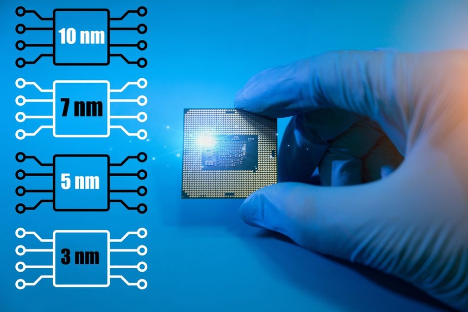
| 300mm (12 in) | < 10 nm (FinFET); typical nodes at 5 nm, 3 nm, etc. | CPUs, GPUs, DRAM, NAND flash, advanced SoCs | Enables high transistor counts and large die size; essential for sub-10 nm and EUV lithography; requires advanced process control and high capital investment. |
Beyond node compatibility, 300mm wafers support larger die sizes—up to ~450 mm² for microprocessors—while 200mm wafers are typically limited to ~320 mm². This constraint arises not only from available surface area but also from yield limitations, as defect probability increases with die size.
Manufacturing challenges and process control
Handling and Automation
Scaling from a 200mm wafer to a 300mm wafer introduced new challenges in wafer handling, transportation, and automation. A 300mm wafer is significantly larger and heavier, with greater thickness to maintain structural integrity. This makes manual handling impractical and increases risks of warpage, breakage, or particle contamination during processing.
To address these issues, 300mm fabs adopted automation-first manufacturing models. Instead of human operators moving wafers, 300mm facilities rely on robotic arms, conveyor systems, and Front Opening Unified Pods (FOUPs) to transport wafers between tools in a sealed, contamination-free environment. FOUPs enable “single wafer” handling, reducing particle exposure and improving yield stability compared with batch cassettes used in older 200mm fabs.
This automation reshaped the economics of a wafer fab. While it required substantial upfront investment in robotic infrastructure, automated wafer transport reduced labor costs, standardized wafer orientation, and improved throughput across production lines. Automated handling is also critical to scaling substrate quality control, since larger wafer sizes magnify the impact of even small misalignments or surface defects.
The transition to automated 300mm fabs represented a pivotal moment for the semiconductor industry, as it allowed higher yields at advanced process nodes while ensuring consistency across high-volume manufacturing. Meanwhile, 200mm fabs continue to rely more heavily on operator interaction, reflecting their focus on mature, less fragile processes where full automation is not economically necessary.
Thermal and Mechanical Properties
Scaling from a 200mm wafer to a 300mm wafer has profound thermal and mechanical implications for semiconductor manufacturing. Larger wafer sizes increase thermal mass, mechanical stress, and defect sensitivity, forcing fabs to adopt new equipment designs and process controls.
Thermal Mass and Heating Time: The heat capacity of a wafer scales with its volume. A 300mm wafer requires ~1.7× longer than a 200mm wafer to reach processing temperatures, as observed in thermal ramp studies. This delay affects cycle times, wafer throughput, and overall fab efficiency. Engineers must adjust ramp rates, dwell times, and thermal budgets to maintain device uniformity across the wafer.
Sagging and warpage: The mechanical stress on larger wafer sizes increases the risk of gravitational sagging and warping during processing. To maintain planarity, 300mm wafers often use thicker substrates (~775 µm versus ~725 µm for 200mm wafers) and employ specialized edge support structures. Wafer chucks, deposition chambers, and lithography stages in 300mm fabs must be redesigned to control mechanical stress and suppress wafer warp.
Surface quality and defects: Because a 300mm wafer provides 2.25× more surface area, even minor imperfections can amplify defect density across the wafer. The raw material cost of a 300mm wafer is about three times higher than a 200mm wafer, making defect control essential to protect yield and reduce manufacturing costs. Advanced process control (APC) techniques such as run-to-run feedback, endpoint detection, and real-time fault monitoring are required to maintain high overall equipment efficiency (OEE). Integrated metrology sensors embedded in modern wafer fabs help minimize defect propagation across production lines.
Equipment Scaling and Cleanroom Infrastructure
The shift to 300mm fabs required extensive re-engineering of lithography, etching, deposition, and metrology tools. Stepper field sizes remain fixed, meaning that more exposures are needed to cover the larger wafer diameter, which increases lithography cycle time. At advanced process nodes, EUV lithography for 5 nm and 3 nm requires vacuum-compatible FOUPs and ultra-clean environments, since even small vibrations or particle contamination can compromise patterning precision. These stricter cleanroom standards raised both capital investment and operating complexity for 300mm wafer fabs.
Material Supply and Substrate Quality
Producing defect-free 300mm silicon wafers places extreme demands on crystal growth. The larger diameter requires Czochralski furnaces capable of pulling longer, more uniform boules with tight control of oxygen content, dopant levels, and thermal gradients. Wafer suppliers must also improve annealing steps to minimize dislocations, slip lines, and oxygen precipitates. These refinements are critical, since poor substrate quality would multiply defects across billions of transistors patterned onto a single die.
Economic and strategic considerations
Capital Investment and Risk
Building and operating a wafer fab is among the most capital-intensive undertakings in the semiconductor industry. The investment required varies drastically between 200mm and 300mm fabs, shaping which companies can participate at each level of manufacturing.
200mm wafer fabs: These facilities have significantly lower startup costs, typically under $2 billion, and often make use of refurbished equipment. Payback periods are shorter, making them attractive to specialty foundries and integrated device manufacturers (IDMs) focused on analog, MEMS, power devices, and mixed-signal ICs. The resurgence of automotive and IoT demand has renewed investment in new 200mm fabs, particularly for SiC and GaN power devices, where mature nodes are sufficient.
300mm wafer fabs: By contrast, a leading-edge 300mm fab can require more than $20 billion in capital outlay. Advanced EUV lithography systems alone can exceed $150 million per tool. The scale of investment introduces substantial financial risk, which only a handful of global giants—Intel, TSMC, Samsung, and AMD—can manage. These fabs enable cutting-edge process nodes (5 nm, 3 nm) and support high-volume production of CPUs, GPUs, DRAM, and other processors, but profitability depends on sustained demand from smartphones, data centers, and AI.
Risk profile: Larger wafer sizes bring lower manufacturing costs per die but increase exposure to supply chain shocks, yield ramp delays, and technology shifts. A 300mm fab is viable only if demand for state-of-the-art nodes remains strong enough to amortize the massive capital outlay. Conversely, 200mm fabs face lower financial risk, but their limitation to mature process nodes constrains their role in cutting-edge logic.
The contrast in capital intensity explains why 300mm fabs are concentrated among a few dominant foundries, while 200mm fabs are widely distributed across niche and regional players. Together, they reflect the trade-off between risk and return that continues to shape global semiconductor manufacturing.
Market Dynamics and Supply Chain
The global semiconductor supply chain depends on a delicate balance between mature 200mm fabs and advanced 300mm fabs, each serving distinct markets but facing unique pressures.
200mm wafer demand: Despite being tied to mature nodes (28–90 nm), demand for 200mm wafers continues to grow. Automotive electronics, analog ICs, MEMS, and IoT devices rely heavily on these wafers because they require long lifecycles, proven reliability, and cost-effective manufacturing. Analysts project more than 12 new 200mm fabs will come online between 2023 and 2026 to meet this demand, though expansion is limited by a shortage of refurbished 200mm equipment in the supply chain.
300mm wafer capacity: Most new fabs being built in the United States, Europe, Taiwan, and China are 300mm fabs, driven by demand for CPUs, GPUs, DRAM, NAND flash, and AI processors. These fabs focus on leading-edge process nodes (7 nm, 5 nm, 3 nm), but utilization rates can fluctuate when demand for smartphones or data centers softens, creating potential bottlenecks in capital recovery.
Supply chain pressures: Equipment scarcity is a growing issue: there are estimated to be only ~500 available 200mm tools compared to a demand of 2,000–3,000. This shortage raises prices and limits fab expansion. Meanwhile, advanced 300mm tools such as EUV lithography systems face long lead times and high costs, further concentrating access among dominant chipmakers like TSMC, Intel, Samsung, and AMD.
Geopolitical factors: Recent disruptions in the semiconductor supply chain, including the COVID-19 pandemic and geopolitical tensions, have accelerated government initiatives such as the U.S. CHIPS Act and the European Chips Act. These policies fund both 200mm fabs (for automotive and industrial security) and 300mm fabs (for cutting-edge logic and memory), reinforcing the complementary role of both wafer sizes in the global semiconductor industry.
Together, these dynamics illustrate why larger wafer sizes like 300mm dominate advanced nodes, while 200mm fabs remain indispensable for high-volume, specialty markets. The supply chain now depends on maintaining both capacities to ensure resilience and balanced growth.
Cost per Wafer vs. Cost per Area
When evaluating wafer economics, it is critical to distinguish between the cost of an entire wafer and the cost per unit area or cost per die.
Cost per wafer: A raw 300mm wafer typically costs 2.5–3× more than a 200mm wafer, reflecting the higher demands of crystal growth, defect control, and handling. The increased manufacturing costs are significant, especially given the higher fragility and processing complexity of larger wafer sizes.
Cost per area: Because wafer area scales with the square of diameter, a 300mm wafer provides 2.25× the surface area of a 200mm wafer. This means that the cost per mm² is lower, making it more efficient for producing high volumes of dies.
Cost per die: For a given die size, the economics of a larger wafer size become clear: more dies per wafer, lower cost per chip. For example, at a 15 mm × 15 mm die, a 200mm wafer yields ~139 dies, while a 300mm wafer yields ~314. Even if the yield is slightly lower on larger wafers, the net number of good dies is higher, reducing per-die cost.
Design dependency: Actual cost efficiency depends on more than wafer diameter. Die size, defect density, process node, packaging, and testing costs all influence the final economics. For high-performance CPUs and GPUs with large die sizes, 300mm wafers are indispensable. For analog, MEMS, and automotive ICs with smaller dies, 200mm wafers remain cost-competitive.
In short, while 300mm wafers appear more expensive upfront, their scaling advantage in area and die per wafer makes them more economical at high volume. This cost trade-off is a cornerstone of modern semiconductor manufacturing strategy, shaping which fabs, processes, and applications are tied to each wafer size.
Applications and design considerations
Despite the industry’s shift to larger wafer sizes, the 200mm wafer remains essential in modern semiconductor manufacturing. Its strength lies in supporting mature process nodes (28–90 nm) that are well-optimized for cost, yield, and reliability.
Devices Suited to 200 mm Wafers
200mm wafers dominate analog and mixed-signal ICs, power management chips, RF transceivers, MEMS sensors, and microcontrollers. Many automotive control units, industrial controllers, and IoT devices are built on nodes between 90 nm and 28 nm, which provide proven reliability, long product lifetimes, and lower non-recurring engineering (NRE) costs. According to Data Bridge Market Research, the growth of electric vehicles and IoT is driving renewed investment in 200mm fabs. Engineers in these domains typically optimize for cost per wafer, yield stability, and supply chain resilience rather than pushing for maximum transistor density.
Devices Suited to 300 mm Wafers
300mm wafers are indispensable for advanced CPUs, GPUs, AI accelerators, DRAM, NAND flash, and high-end SoCs, where transistor counts can exceed tens of billions. WaferPro notes that 300mm wafers support sub-10nm FinFET nodes and allow die sizes of up to ~450 mm², making them essential for high-performance computing, smartphones, 5G base stations, and data center processors. Engineers designing on these nodes must contend with EUV lithography constraints, thermal design power, and advanced packaging technologies such as 2.5D interposers and 3D stacking.
Mixed Strategies and Multi-project Wafers
Some products span both wafer sizes. For example, a heterogeneous SoC may combine a high-performance logic core on a 300mm wafer with analog or power domains fabricated on a 200mm wafer, later integrated through chiplet-based packaging. In addition, multi-project wafer (MPW) programs allow startups, universities, and small design teams to share a 300mm fab run, reducing NRE costs while gaining access to advanced process nodes.
Mixed strategies and multi‑project wafers
Some products may span both wafer sizes. For example, a system-on-chip with a high-performance core and multiple analog or power domains could be implemented as separate chips, fabricated on 300 mm and 200 mm wafers, and later integrated via package-level interconnect (chiplet approach). Multi‑project wafer (MPW) programs also allow small teams to prototype on shared 300 mm wafers, reducing NRE costs.
Recommended reading: The Ultimate Guide to Wafer Dicing: Techniques, Challenges, and Innovations
Future Trends and Outlook for 450 mm Wafers
The semiconductor industry has explored 450 mm (18-inch) wafers, but widespread adoption has stalled due to escalating lithography costs, scaling complexities, and uncertain economic benefits. Increasing wafer size from 200 mm to 300 mm yields a 2.25× increase in die area and roughly a 30% reduction in cost per chip. In contrast, scaling from 300 mm to 450 mm offers only a 1.96× area increase, making the return on investment less compelling.
Technical challenges are significant: 450 mm wafers weigh nearly four times a 200 mm wafer, requiring major modifications in handling equipment and robotics. Tool scaling is non-trivial; uniform thermal management across the larger surface becomes more difficult, and capital expenditures for fabrication facilities rise sharply.
Current industry roadmaps prioritize maximizing 300 mm wafer productivity through advanced process nodes, improved yield, and 3D integration technologies such as chiplets and stacking, rather than further diameter increases. Most analysts expect 300 mm wafers to remain the standard through the 2030s, with 450 mm used only for selective experimental or niche applications.
Conclusion
Wafer size remains a critical factor in semiconductor manufacturing. 200 mm wafers offer a mature, cost-effective platform for analog, power, and embedded applications, providing high yields and rapid return on investment. 300 mm wafers deliver economies of scale for advanced logic and memory, offering 2.25× more surface area, support for sub‑10 nm nodes, and lower cost per chip, despite requiring multi‑billion‑dollar fabrication facilities. The increased area allows a 300 mm wafer to produce over twice as many dies as a 200 mm wafer, underpinning their dominance in high-performance computing.
Looking ahead, while 450 mm wafers remain experimental due to technical and economic challenges, the industry is increasingly focusing on maximizing 300 mm productivity and adopting 3D integration technologies, such as chiplets and stacking, to meet growing demands for higher performance and compact designs. Nonetheless, 200 mm wafers will continue to expand in sectors like IoT, automotive, and power electronics. For engineers and students, choosing between wafer sizes requires understanding geometric scaling, yield behavior, cost trade-offs, and supply-chain dynamics. Both wafer sizes will remain complementary, supporting diverse technologies as the semiconductor industry evolves toward more advanced packaging and integration.
Frequently Asked Questions (FAQ)
What is the primary difference between 200 mm and 300 mm wafers?
The key distinction is wafer size. A 300mm wafer has 2.25× the surface area of a 200mm wafer. This larger area supports more dies per wafer—roughly double—reducing cost per chip when a 300mm fab runs at full capacity.Why are 200 mm wafers still widely used?
Not all devices require cutting-edge nodes. Analog ICs, MEMS, RF, and power devices perform well on mature 200mm fabs, which offer high yield, lower capital intensity, and access to refurbished equipment. Market forecasts project strong growth in 200mm capacity between 2023 and 2026, driven by automotive and IoT demand.How much cheaper is a die from a 300 mm wafer?
Scaling wafer diameter from 200mm to 300mm can reduce manufacturing costs per die by about 40%. In practice, 300mm fabs deliver around 1.7× lower cost per chip when operating at high utilization. However, capital costs are far higher: a leading-edge 300mm fab exceeds $20 billion, compared with under $2 billion for a 200mm fab.Can a 200 mm fab be upgraded to 300 mm?
No. A 300mm wafer is larger and heavier, requiring redesigned process tools, automation systems, FOUP carriers, and cleanroom layouts. The conversion demands entirely new infrastructure and R&D investment, making retrofitting impractical.Which process nodes are supported?
200mm wafers: Mature 28–90 nm nodes, used for MCUs, analog ICs, MEMS, and power management devices.
300mm wafers: Advanced sub-10 nm nodes (5 nm, 3 nm), supporting CPUs, GPUs, DRAM, NAND, and high-performance SoCs.
Does a larger wafer always mean higher yield?
Not initially. Larger wafer sizes increase the probability of defects, lowering yield. Over time, as process nodes mature and fabs deploy advanced process control (APC) techniques, yields on 300mm wafers approach those of 200mm wafers.Will 450 mm wafers replace 300 mm?
The industry investigated 450mm wafers, which offer nearly twice the area of 300mm. However, predicted cost savings of only 10–30% did not justify the massive tooling and fab investment. Most analysts expect 300mm wafers to remain the standard through the 2030s, while 450mm research continues quietly in the background.
Additional Resources
Die‑Per‑Wafer calculators: Online tools help estimate gross and net die count for various die sizes and wafer diameters. They account for edge losses and scribe lines, providing more accurate yield predictions than simple area ratios.
Semiconductor Equipment and Materials International (SEMI): SEMI regularly publishes reports on wafer fab outlook, capacity trends, and equipment markets. Their 200 mm fab outlook provides detailed statistics on planned expansions and regional breakdowns.
Industry roadmaps: Organizations like the IEEE International Roadmap for Devices and Systems (IRDS) release roadmaps covering process nodes, wafer sizes, lithography, and packaging trends. These resources help engineers anticipate future technology shifts and plan long‑term investments.
References
Microchip USA, "200mm vs 300mm Silicon Wafers," Microchip USA, Feb. 21, 2025. [Online]. Available: https://www.microchipusa.com/electrical-components/200mm-vs-300mm-silicon-wafers. [Accessed: Aug. 11, 2025].
Data Bridge Market Research, "Global Silicon Wafer Reclaim Market," Data Bridge Market Research, Jul. 2021. [Online]. Available: https://www.databridgemarketresearch.com/reports/global-silicon-wafer-reclaim-market. [Accessed: Aug. 11, 2025].
S. Bajikar, "How to Think About Rising WFE Intensity," Applied Materials, Jan. 28, 2022. [Online]. Available: https://www.appliedmaterials.com/us/en/blog/blog-posts/how-to-think-about-rising-wfe-intensity.html. [Accessed: Aug. 12, 2025].
S. Davis, "Silicon Wafers Market on Track for Growth," Semiconductor Digest, Mar. 6, 2025. [Online]. Available: https://www.semiconductor-digest.com/silicon-wafers-market-on-track-for-growth/. [Accessed: Aug. 13, 2025].
Isel USA, "Wafer Handling Robots," Isel USA, [Online]. Available: https://www.isel-us.com/wafer-handling-robots. [Accessed: Aug. 14, 2025].
A. Abiola, “PCB Assembly Services: Market Size, Share, Trends, and Forecast,” NextPCB Blog, Aug. 19, 2025. [Online]. Available: https://www.nextpcb.com/blog/pcb-assembly-services-market-size-share-trends-and-forecast [Accessed: Aug. 20, 2025].
in this article
1. Key Takeaways2. Introduction3. Evolution of Wafer Sizes4. Manufacturing Efficiency and Cost5. Manufacturing challenges and process control6. Economic and strategic considerations7. Applications and design considerations8. Future Trends and Outlook for 450 mm Wafers9. Conclusion10. Frequently Asked Questions (FAQ)11. Additional Resources12. References