How to maximize the yield in wafer production webinar
Join MVTec to explore how advanced machine vision software is revolutionizing semiconductor wafer inspection with live demos, not slides—boosting precision, quality, and efficiency.

08 May, 2025.
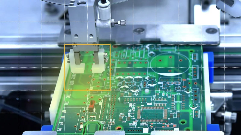
Detecting defects on semiconductor wafers is extremely challenging due to their reflective surfaces, micro-scale defects, and the need for high precision. Manual parameter tuning and traditional rule-based approaches can be time-consuming and inconsistent, especially when scaling across varying product lines. Machine vision software is therefore playing an increasingly critical role in semiconductor manufacturing, by enabling automated, robust, and highly efficient optical inspection processes.
Join MVTec on June 5th for a step-by-step, demo-driven webinar and discover how advanced vision technologies are transforming wafer inspection and driving quality as well as throughput in semiconductor manufacturing.
Discover a smarter way to detect wafer defects – no slides, just solutions.
What You’ll Learn
How Machine Vision can be used to detect defects on a wafer showing a live demo
Which technologies in MVTec HALCON can be used to maximize the yield
How MVTec can support you to start with an automated optical inspection
 | Moderator Markus Setzer has been a Marketing Specialist at MVTec for six years. In his role at MVTec, he talks a lot with customers and interested parties. Through trade fairs in particular, he has a deep insight into the industry's most pressing questions regarding machine vision in production. The demands of the market shape the structure of the webinar, which Markus Setzer will moderate. |
Application Engineer Coco Rogers works as an Application Engineer in the Customer Service department and brings extensive expertise in defect detection. She has in-depth knowledge of the semiconductor industry and also develops demonstrators that showcase our software in action. During the webinar, Coco will give a live demonstration of how the optical inspection process of a wafer is performed using advanced machine vision technologies. |  |
About MVTec
MVTec develops machine vision software used across a wide range of industrial applications, including semiconductor manufacturing. Its tools support tasks such as wafer alignment, inspection of dies and ball/wire bonds, defect classification, shape matching, precise measurement in 2D and 3D, as well as 3D robot guidance and identification. These capabilities contribute to improving production efficiency, enabling advanced manufacturing processes, and supporting applications where human-machine collaboration is required.