Thin Film Deposition: Everything You Need to Know
Thin film deposition is a process used to create thin film coatings on different materials. Thin films can consist of metal, semiconductors, and dielectrics, providing them with different properties. These properties translate to benefits such as electrical insulation, optical transmission, and corrosion resistance, that can be used to improve substrate performance. This article explores the processes of thin film deposition, along with its types, parameters, benefits, drawbacks, and applications.

21 Mar, 2023. 12 minutes read
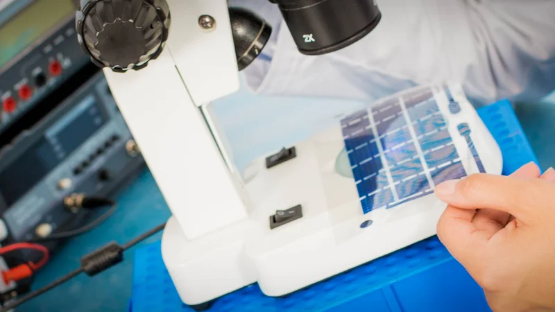
Thin Film Solar Cell
Introduction
Thin film deposition technology involves coating the surface of a substrate with a very thin film of material that ranges in thickness from a few nanometers to 100 micrometers, or just a few atoms. It can also be used to build up layers on top of already-deposited coatings. Thin film deposition technology or manufacturing processes have become integral to the development of modern electronics such as semiconductors, optical devices, solar panels, disk drives, CDs, etc. Thin film coatings can be applied using a variety of technologies and techniques, which can be efficiently deployed using an array of tools and equipment that enhance the process.
Thin Film Deposition: Definition and Importance
Thin film deposition is a process where thin film coatings are produced and deposited onto a substrate material. Many different materials can be used to create these coatings, including metals, oxides, and compounds. Additionally, thin film coatings have a variety of traits that can be used to change or enhance a particular aspect of the performance of the substrate. For instance, some are transparent, others are powerful and scratch-resistant, and still, others alter the conductivity of electricity or signal transfer.
Thin films are typically used to improve the surface properties of solids or bulk materials. These properties include but are not limited to transmission, reflection, absorption, hardness, abrasion resistance, corrosion, permeation, and electrical behavior. Hence, it is an important manufacturing step in the production of many solid-state, optoelectronic, and medical devices and products, including consumer electronics, precision optics, compound semiconductors, semiconductor lasers, fiber lasers, microscopy & microanalysis sample slides, LED displays, optical filters, medical implants, and even nanotechnology.
Thin Film Deposition is broadly divided into two categories: Chemical Deposition and Physical Vapor Deposition Coating Systems.
Basic Principles of Thin Film Deposition
The technique used to produce thin films, such as evaporation, sputtering, ion beam deposition, or chemical vapor deposition, determines the production process. In each case, the determinant of a suitable thin-film creation method is the application, the target and substrate materials, the required uniformity of the film, as well as chemical and physical properties, such as corrosion resistance or high thermal conductivity.
To illustrate, while sputtering is often the most effective method for creating coatings to enhance optical qualities, thin-film polycrystalline silicon, which is frequently used in integrated circuits, works well with chemical deposition. There is no perfect universal system or technique for thin film deposition. The chosen technique and configuration will rely on the specific performance and output requirements for a particular application. [1]
Types of Thin Film Deposition Techniques
There are many techniques and sub-techniques of thin film deposition. This section adequately discusses them.
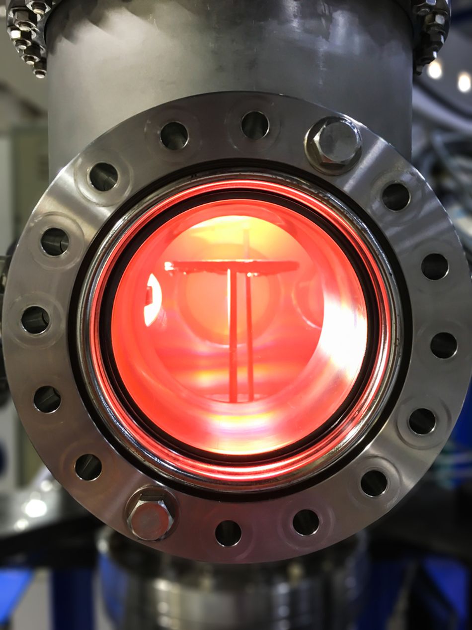
Physical Vapor Deposition (PVD)
Physical vapor deposition (PVD) refers to a range of thin film deposition techniques that involve vaporizing a solid material in a vacuum, then depositing that material onto a substrate using mechanical, electromechanical, or thermodynamic processes. The surface of a material source is physically vaporized into gaseous atoms, and molecules, or partially ionized into ions under vacuum conditions. Then, a film having a specific function is deposited on the surface of the substrate by a low-pressure gas (or plasma). PVD film has fast deposition speed as well as strong adhesion; therefore coatings that are created in this manner are highly durable. They are also scratch and corrosion-resistant. PVD has a wide application range, from solar cells to eyeglasses to semiconductors.
(i). Evaporation
The evaporative deposition technique falls under the PVD umbrella, and it consists of the following types:
E-beam evaporation (electron beam): This process involves using a highly-charged electron beam to evaporate the intended material. After which the evaporated material is deposited onto the substrate, thereby creating a thin film with the atoms formed. This process is usually applied for optical thin films such as glasses and solar panels.
Thermal evaporation: Here the intended material is heated by a resistive heat source until it generates vapor pressure. The thin film is then created when the evaporated material coats the substrate. This form of PVD is used to deposit metals for thin film transistors, solar cells, and OLEDs.
Ion-assisted deposition (IAD): This technique can be used with either sputtering or thermal evaporation processes to produce high-quality films with remarkable precision. An ion beam is directed at a substrate while a PVD coating is applied in a high vacuum environment. This facilitates process control, producing films with less scatter than conventional evaporation. The IAD technique is also called Ion Assisted Coating (IAC), Ion Beam Enhanced Deposition (IBED), Ion Beam Sputtering (IBS), and Ion Vapor Deposition (IVD), but the most common is Ion Beam Assisted Deposition (IBAD)
(ii). Magnetron Sputtering
Magnetron sputtering is also subsumed under PVD. It is a plasma-based deposition technique involving a gaseous plasma that is generated and magnetically confined to a space containing the target material to be deposited. High-energy ions within the plasma collide with the surface of the target material and the liberated atoms travel through the vacuum environment and are sputtered or deposited onto a substrate to create a thin film. This technology is commonly used to make insulating or metallic coatings for optical and electrical purposes.
(iii). lon Beam Sputtering
Ion beam sputtering (IBS) is one of the realizations of Ion Assisted Deposition, discussed above. It is also called ion beam deposition (IBD). In this process, an ion source is used to sputter the target material onto the substrate, creating a thin film. These kinds of thin films are known to have high quality, and precise thickness due to the monoenergetic ion beam used.
(iv). Pulsed Laser Deposition (PLD)
Pulsed laser deposition is a type of evaporation process that uses high-power laser pulses to vaporize the target material within the vacuum chamber. The laser beam produces a plume of plasma which is deposited as a thin film on a substrate. The PLD process involves evaporation, ablation, plasma formation, and exfoliation, making it more complicated than other methods, but it has proven beneficial due to its high deposition rates and streamlined process.
Chemical Vapor Deposition (CVD)
Chemical Vapor Deposition, commonly referred to as CVD, refers to a group of thin film deposition techniques that use plasma or thermally induced chemical reactions to produce dense thin films at the surface of a substrate. These reactions may involve the substrate material itself but often do not. For thermal CVD, the processes are run at elevated temperatures and atmospheric or lower pressures.
A wide variety of CVD processes are widely used for producing high-quality, high-performance solid coatings or polymers.
(i). Atmospheric Pressure CVD
Atmospheric Pressure CVD (APCVD) is a deposition technique carried out at atmospheric pressure (normal pressure) To achieve the decomposition and combination reactions in this method, extremely high temperatures are required. The applied gases are decomposed and react with each other to form the desired film. The process typically requires temperatures from 1000-1300C.
(ii). Low-Pressure CVD
In this type of chemical vapor deposition, gas is drawn out through the deposition chamber with a vacuum pump. This combined with the furnace tube decreases the pressure of the process gases, which allows a reaction at lower temperatures than atmospheric pressure CVD. Low pressure facilitates a more uniform deposition rate with reduced gas-phase reactions.
(iii). Ultrahigh Vacuum CVD
In the ultra-high vacuum technique, known as UHV/CVD, one or more volatile precursors interact with a substrate under ultra-high vacuum (<10^{-6} Pa). This causes a reaction or decomposition on the surface of the substrate, creating a deposit. Gas transport in this technique is achieved by molecular flow since the process requires pressures below 10-6 Pa (10-8 Torr). In addition, the low frequency of molecular collisions ensures that there is no gas-phase chemistry involved.
(iv). Atomic Layer Deposition
Atomic layer deposition (ALD) is a process for depositing highly uniform thin films. It also enables precise thickness control with easily replicable results. It involves alternating exposures of a substrate surface to vapors of two chemical reactants. The next coating is then introduced into the chamber to create high-quality thin films that are easy to control.
ALD deposits films layer by layer by employing alternating, saturation reactions between gaseous precursor molecules and a substrate. Repeating this sequential reaction allows for the precise deposition of films of nearly any thickness, be they atomic monolayers or micrometer-sized. This approach of alternating reactions does away with the line-of-sight and constant-exposure specifications that restrict more traditional techniques like physical or chemical vapor deposition.
(v). Plasma-Enhanced PIB-CVD
Plasma-enhanced CVD is an alternative to standard CVD that requires a lower temperature. It can create, for example, high-quality silicon dioxide (SiO2) film at 300°C to 350°C as opposed to the temperature range of 650°C to 850°C required by standard CVD to create similar films. cold plasmas are introduced to the deposition chamber to increase the deposition particle's electron temperatures. In this method, two reactive gases are combined to form a plasma. This triggers a chemical reaction that causes the deposition of a thin film onto the substrate. [2]
Others
There are many other forms of CVD in wide use. These processes are differentiated by their process conditions and how the chemical reactions are initiated.
Aerosol-assisted CVD (AACVD) - A CVD process in which the precursors are transported to the substrate through a liquid/gas aerosol, which can be ultrasonically generated.
Direct liquid injection CVD (DLICVD) - A CVD process in which the precursors are in liquid form.
Hotwire CVD (HWCVD) - Also known as Catalytic CVD (Cat-CVD) or hot filament CVD (HFCVD). Applies a hot filament to chemically decompose the source gases.
Metalorganic chemical vapor deposition (MOCVD) - CVD processes based on metalorganic precursors.
Hybrid Physical-Chemical Vapor Deposition (HPCVD) - Vapor deposition processes that involve both physical evaporation of solid source and chemical decomposition of precursor gas.
Rapid thermal CVD (RTCVD) - CVD processes that use heating lamps or other methods to quickly heat the substrate. When the substrate alone is heated instead of the gas or chamber walls, unwanted gas phase reactions that can lead to particle formation are reduced.
Materials used for Thin Film Deposition
Metals, oxides, and compounds are some of the materials that are most frequently employed in thin film deposition. In each case, these materials have specific advantages and disadvantages that inform their selection. Metals are good for thermal and electrical conduction, oxides offer protection, and compounds can be specially made to have specific properties. The choice of material for a thin film coating ultimately depends on the requirements of the application it is being used for.
Metals
Metals are often employed in thin film deposition due to their strength and durability Moreover, they are simple to deposit onto a substrate material, making them a preferred option for most applications. Metals can, however, be rather pricey, which may restrict their use in particular applications.
Oxides
Another prominent option for thin film deposition is oxides. They are frequently employed because they are tough and resistant to high temperatures. They are a useful option for numerous applications because they can also be deposited at relatively low temperatures. Oxides can, however, be brittle and challenging to work with, which can sometimes limit their application.
Compounds
In thin film deposition, compounds are chosen for a variety of reasons. They can be deposited at relatively low temperatures, demonstrating strength and durability. This makes them suitable for many applications. However, compounds can also be costly and challenging to work with, which sometimes limits their use. [3]
Key Parameters and Factors Affecting Thin Film Deposition
Deposition Rate
This is a measurement of how quickly the film is produced. It typically utilizes units of thickness divided by time. It is crucial to pick a technology with a deposition rate appropriate for the applications.
For thin films, one can use a relatively moderate deposition rate, and for thick films, a quick deposition rate. The goal is to retain control and strike a balance between the demands of speed and accurate film thickness control.
Uniformity
This is a measure of film consistency across a substrate. Usually, it refers to film thickness but it can also refer to other film properties such as index of refraction. It is useful to have a good understanding of the application to avoid over or under-specifying uniformity.
This is an assessment of the consistency of film across a substrate. It usually relates to film thickness, but it can also be used to describe other film characteristics, such as the index of refraction. It is helpful to have a solid grasp of the application to avoid specifying a consistency that is too low or too high.
Fill capability
Fill capability or Step coverage are terms used to indicate how well a deposition process covers the topography of the substrate. Step coverage is calculated as the ratio of the deposited film thickness in the open area without features to the deposited thickness along the sidewalls or bottom of the features. The deposition method (such as CVD, PVD, IBD, or ALD) has a significant impact on the step coverage and fill.
Film characteristics
The characteristics of a film are application-dependent. The application requirements can be roughly divided into categories like photonic, optical, electronic, mechanical, or chemical. Most times, films must meet requirements in more than one category.
Process Temperature
Process temperature significantly affects film characteristics. The application can impose limits on the temperature that can be used.
Damage
Each deposition technology has the potential to inflict damage on the material being deposited upon and as features get increasingly smaller, they usually become more vulnerable to process damage. There could be several simultaneous sources of damage, such as pollution, UV radiation, or ion bombardment. It's critical to comprehend the limitations of your materials and tools. [4]
Applications of Thin Film Deposition
Discussed in this section are some types of thin films in terms of their applications:
Zinc Oxide-Based Thin-Film
These are found in several industries, including thermal, optical, magnetic, and electrical. However, the primary applications of ZnO thin films are coatings and semiconductor devices.
Thin Film Resistor
Modern technology makes extensive use of thin-film resistors, which are essential for many thin-film applications. It can be used for a variety of things, including radio receivers, circuit boards, computers, and radiofrequency devices. They are also extremely useful in monitors, wireless routers, Bluetooth modules, and cell phone receivers.
Magnetic Thin Film
Electronics, data storage, radio-frequency identification, microwave devices, displays, circuit boards, and optoelectronics all depend on magnetic thin films as key components.
Optical Thin Films
Optical coatings and optoelectronics are examples of standard applications of optical thin films which offer an array of uses. Manufacturers can use molecular beam epitaxy to produce optoelectronic thin-film devices (semiconductors). In MBE, epitaxial films are produced by depositing one atom at a time onto the substrate.
Polymer Thin Film
Polymer thin films are used in a variety of products, including memory chips, solar cells, and electronic devices. Modern chemical deposition techniques (CVD) provide more precise control of polymer film coatings, including conformance and coating thickness.
Thin-Film Battery
Many of the electronic devices in use today are powered by rechargeable batteries, such as the lithium-ion battery, which has advanced greatly thanks to the use of thin films. The powering of implantable medical devices is another use for thin-film batteries in the healthcare sector.
Thin-Film Coating
Several industries and technological fields can benefit from thin-film coatings. Manufacturers utilize coating methods during deposition to enhance the chemical and mechanical characteristics of target materials. Anti-reflective coatings, anti-ultraviolet or anti-infrared coatings, anti-scratch coatings, and lens polarization are some common examples.
Thin-Film Solar Cells
Thin-film solar cells are essential to the solar energy industry because they enable the production of relatively cheap, and clean electricity. Photovoltaic systems and thermal energy are the two main technologies applicable. [5]
Advantages and Disadvantages of Thin Film Deposition
Some of the most common benefits of thin films include improved adhesion, corrosion and wear resistance, and increased durability. Moreover, thin films can offer a variety of aesthetic advantages, such as enhancing a substrate's appearance or making it more reflective. Generally, thin film deposition presents many benefits and can be tailored to enhance a substrate's performance.
Here are the benefits and drawbacks from the perspective of the two main divisions of thin film deposition.
CVD Advantages
- Ability to generate highly pure and dense films or small particles at relatively high deposition rates.
- Capacity to uniformly coat components with complex shapes due to their non-line-of-sight nature.
- CVD can deposit a variety of metallic, ceramic, and semiconducting thin films.
Disadvantages of CVD
- It is difficult to synthesize multi-component materials by CVD because of fluctuations in vapor pressure, nucleation, and growth rates during the gas-to-particle conversion. This leads to the heterogeneous composition of particles.
- In thermally activated CVD, there are no extremely volatile, toxic, or pyrophoric precursors. [6]
PVD Advantages
- PVD coatings can be more durable and resistant to corrosion than coatings applied using the electroplating procedure.
- Ability to apply nearly any sort of inorganic and some organic coating material utilizing a wide range of finishes to a wide range of substrates and surfaces.
- Most coatings have exceptional abrasion resistance, high temperature, and good impact strength, and are so long-lasting that protective topcoats are practically never required.
- Less harmful to the environment than conventional coating techniques like electroplating and painting.
- A film can be deposited using more than one method.
PVD Disadvantages
-Some PVD technologies require vacuums and operate at extremely high temperatures, necessitating specific care from operating people.
-Specific technologies can impose limitations on the process.
-A cooling water system is necessary to dissipate heavy heat loads. [7]
Key Takeaways
Thin film deposition is a process that is commonly used to make semiconductor devices. It is one of the most important ways of making integrated circuits and is paving the way for the development of nanotechnology. Moreover, its benefits stretch out to many industries as discussed in this article, which further solidifies its relevance to modern technological advancements.
References
1. Denton Vacuum. What is Thin Film Deposition? 2022. [Cited 2023, Mar 17] Available from: https://www.dentonvacuum.com/resources/what-is-thin-film-deposition/#:~:text=Thin%20film%20deposition%20is%20the,metals%20to%20oxides%20to%20compounds
2. VacCoat. Deposition Methods | Vacuum Deposition. 2021. [Cited 2023 Mar 17] Available from: https://www.google.com/amp/s/vaccoat.com/blog/deposition/%3famp=1
3. AEM. What is Thin Film Deposition? 2022. [Cited 2023 Mar 17] Available from: https://www.aemdeposition.com/blog/what-is-thin-film-deposition.html
4. Coral. Factors that Determine Deposition Performance. 2022. [Cited 2023 Mar 17] Available from: https://www.google.com/amp/s/corial.plasmatherm.com/en/blog/factors-that-determine-deposition-performance%3fhs_amp=true
5. Korvus Technology. Thin Film Applications in Various Fields. 2022. [Cited 2023 Mar 18] Available from: https://korvustech.com/thin-film-applications/
6. SiloTek. Chemical Vapor Deposition: Benefits and Limitations. 2022. [Cited 2023 Mar 18] Available from: https://www.google.com/amp/s/www.silcotek.com/blog/chemical-vapor-deposition-benefits-and-limitations%3fhs_amp=true
7. Atria Innovation. Physical Vapor Deposition (PVD) 2021. [Cited 2023 Mar 18] Available from: https://www.google.com/amp/s/www.silcotek.com/blog/chemical-vapor-deposition-benefits-and-limitations%3fhs_amp=true
in this article
1. Introduction 2. Thin Film Deposition: Definition and Importance3. Basic Principles of Thin Film Deposition4. Types of Thin Film Deposition Techniques5. Materials used for Thin Film Deposition 6. Key Parameters and Factors Affecting Thin Film Deposition7. Applications of Thin Film Deposition8. Advantages and Disadvantages of Thin Film Deposition9. Key Takeaways10. References 1. Denton Vacuum. What is Thin Film Deposition? 2022. [Cited 2023, Mar 17] Available from: https://www.dentonvacuum.com/resources/what-is-thin-film-deposition/#:~:text=Thin%20film%20deposition%20is%20the,metals%20to%20oxides%20to%20compounds