Silicon Semiconductor: A Comprehensive Guide to Silicon and its Use in Semiconductor Technology
Silicon has emerged as the most widely used semiconductor material in the electronic industry, paving the way for the digital age. However, many are still oblivious to the unique properties and characteristics that make silicon ideal for a range of applications. This article explores the fundamentals of semiconductor materials, the properties of silicon that make it a prominent player in the semiconductor industry, and its diverse applications in electronic devices.

10 Aug, 2023. 14 minutes read
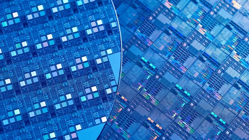
Silicon semiconductor wafer
Introduction
Semiconductors are the backbone of modern electronics, and their development has revolutionized how we live our lives. From smartphones to cars, semiconductors are the critical components that power the devices we rely on every day. And at the heart of these semiconductors is silicon, an element that has played a vital role in the development of modern technology. Silicon i the second most abundant element in the Earth's crust as it makes up about 27.7% of the Earth's crust by mass. Silicon is a chemical element with the symbol Si and atomic number 14. It is a metalloid with both metallic and non-metallic properties. Silicon is widely used in the electronics industry due to its excellent electrical properties, such as a relatively small energy gap or bandgap. It is also used to manufacture solar cells, glass, ceramics, and other materials.
Though gallium arsenide (GaAs) is also a compound semiconductor material that has a higher electron mobility and a higher saturated electron velocity than silicon, silicon is often preferable as it is inexpensive, and has a high melting point, making it ideal for use in high-temperature applications. Silicon also has a unique ability to be doped, which means that it can be intentionally contaminated with other elements to alter its electrical properties. This ability to control the electrical properties of silicon has made it the foundation of modern electronics as it is the most commonly used material in the manufacturing of computer chips or microprocessors. The fabrication process involves the deposition of multiple layers of material, including silicon, to create the necessary components such as transistors, diodes, and resistors. The transistors are used to amplify or switch electronic signals, while the diodes and resistors are used to control the flow of electric current.
The use of silicon in computer chips has enabled the development of high-performance electronic devices with low power consumption, making them suitable for a wide range of applications, including computers, smartphones, and other consumer electronics. The ability to fabricate complex electronic circuits on a small area of silicon has revolutionized the electronics industry, enabling the development of smaller, faster, and more powerful electronic devices. As technology advances, silicon's importance in the industry is only set to grow, making it a critical semiconductor material for the future of electronics.
Basics of Semiconductor Materials
A semiconductor is a material that has electrical conductivity properties between those of a conductor and an insulator. Semiconductors are essential components in electronic devices, as they can be manipulated to control the flow of electrical current. The properties that make a material suitable for use as a semiconductor include its ability to conduct electricity under certain conditions, its temperature-dependent conductivity, and its capacity to be doped with impurities to modify its electrical behavior.
Conductors, Insulators, and Semiconductors
To understand semiconductors, it's important to differentiate them from conductors and insulators. Conductors are materials that allow the free flow of electric current, with low resistance to the movement of electrons. Examples of conductors include metals like copper and aluminum. Insulators, on the other hand, are materials that impede the flow of electric current, having high resistance to the movement of electrons. Examples of insulators include rubber and glass. Semiconductors fall between conductors and insulators in terms of their electrical properties. They have a moderate resistance to the flow of electric current, which can be altered by factors such as temperature, light, and the presence of impurities. The electrical properties of these materials are determined by their atomic structure, specifically the arrangement of electrons in their energy bands.
In conductors, the valence band, which contains the outermost electrons, overlaps with the conduction band, allowing electrons to move freely and conduct electricity. In insulators, there is a large energy gap, known as the bandgap, between the valence and conduction bands, preventing the flow of electric current. Semiconductors have a smaller bandgap, which allows for some electron movement between the valence and conduction bands, enabling them to conduct electricity under specific conditions. The size of the bandgap is a critical factor in determining the behavior of a material as a conductor, insulator, or semiconductor.
Also, thin films are significant materials in the creation of semiconductor devices. Thin films can be used to create conductive and insulating layers, as well as other components of the device. By depositing thin films on a silicon wafer, it is possible to create the various layers and components required to build a semiconductor device. Thin films can be used to create conductors, but not all conductors are made using thin films. For example, copper wire is a conductor that is not made using thin film technology. However, thin films are commonly used to create conductive layers in semiconductor devices and other electronic components.
Thin films can also be used to create insulators, such as silicon dioxide or aluminum oxide. These insulating films can be deposited on a substrate, such as a silicon wafer, to create a layer that prevents the flow of electric current. Thin films are used to create insulating layers in many electronic devices, including transistors and integrated circuits. Thin films are also used to create semiconductors. By depositing thin films of certain materials, such as silicon or germanium, on a substrate, it is possible to create a layer with semiconductor properties. These layers can be used to create the various components of semiconductor devices, including diodes, transistors, and solar cells. Thin films are essential to the creation of modern semiconductor devices.
Further reading: What is a Semiconductor? A Comprehensive Guide to Engineering Principles and Applications
Silicon: A Key Semiconductor Material
Silicon is the most widely used semiconductor material in the electronics industry. Its popularity can be attributed to several factors, including its abundance in the Earth's crust, its ability to form high-quality insulating oxide layers, and its compatibility with various fabrication processes. Silicon's basic properties, such as its temperature-dependent conductivity and its capacity to be doped with impurities, make it an ideal material for a wide range of electronic applications.
Silicon semiconductors are used in a wide variety of devices, including transistors, which are used to amplify and switch electronic signals, integrated circuits, which are used to perform complex functions in electronic devices, and solar cells, which convert sunlight into electricity. The use of silicon in semiconductor manufacturing has revolutionized the electronics industry, making it possible to produce smaller, faster, and more powerful electronic devices.
Silicon's Atomic Structure
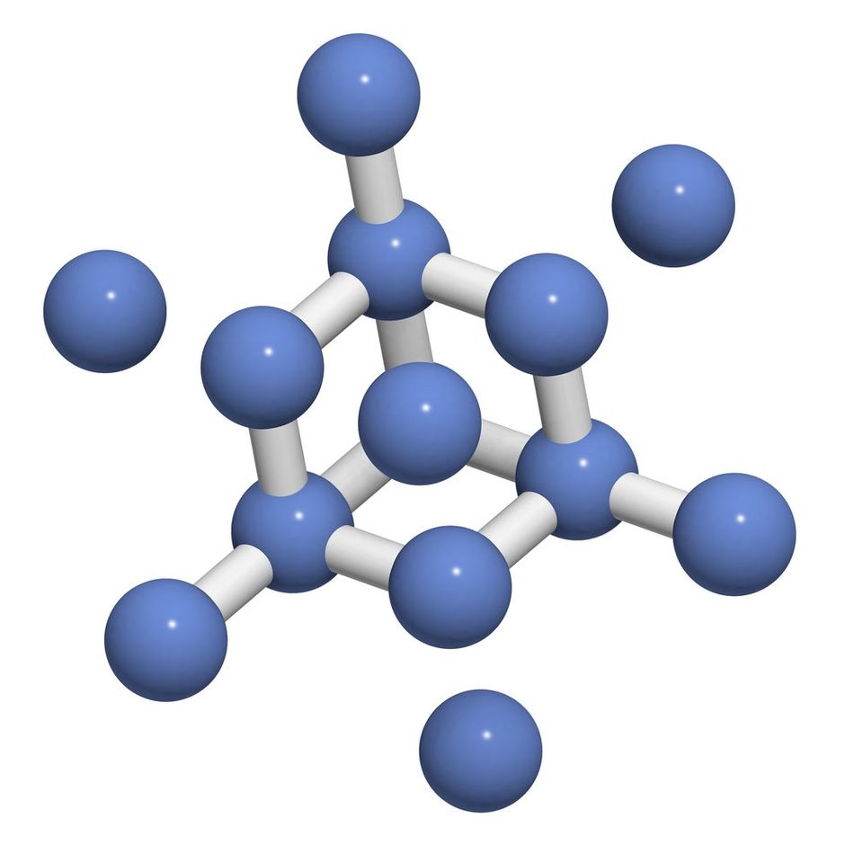
The atomic structure of silicon plays a significant role in its semiconductor properties. Silicon is a tetravalent element, meaning it has four valence electrons in its outermost electron shell. These valence electrons are responsible for forming covalent bonds with neighboring silicon atoms, creating a stable and well-ordered crystal lattice structure.
In a pure silicon crystal, each silicon atom shares its four valence electrons with four neighboring atoms, resulting in a full outer electron shell for each atom. This full outer shell makes it difficult for electrons to move freely within the crystal lattice, giving silicon its intrinsic semiconducting properties. However, when silicon is doped with impurities, its electrical behavior can be altered, allowing for the creation of n-type and p-type semiconductors, which are essential for the functioning of electronic devices such as transistors and integrated circuits.
Silicon's Crystal Structure
The crystal structure of silicon is another important factor that contributes to its semiconductor properties. Silicon forms a diamond cubic crystal lattice, which is characterized by a repeating pattern of atoms in a three-dimensional arrangement. In this structure, each silicon atom is covalently bonded to four neighboring atoms, creating a highly ordered and stable lattice.
The stability and regularity of the silicon crystal lattice play a crucial role in its electrical properties. The well-ordered arrangement of atoms allows for the formation of energy bands, which determine the material's ability to conduct electricity. In silicon, the valence band is separated from the conduction band by a relatively small energy gap, or bandgap, of approximately 1.12 electron volts (eV) at room temperature. This bandgap size is ideal for many electronic applications, as it allows for controlled electron movement between the valence and conduction bands under specific conditions, such as the application of an electric field or the introduction of impurities through doping.
The crystal structure of silicon also has a significant impact on its ability to form high-quality insulating oxide layers. When silicon is exposed to oxygen at high temperatures, it forms a thin layer of silicon dioxide (SiO2) on its surface. This oxide layer acts as an excellent insulator, preventing the flow of electric current between adjacent silicon regions. This property is particularly important in the fabrication of integrated circuits, where the ability to isolate different components on a single silicon chip is essential for proper device operation.
The presence of free electrons in silicon is also important in the operation of electronic devices. By doping the silicon with impurities such as boron or phosphorus, free electrons or "holes" can be introduced into the crystal lattice. The concentration of free electrons or holes determines the electrical properties of the semiconductor, and these properties can be controlled by applying a voltage or current to the device.[1]
Doping Silicon: Creating n-type and p-type Semiconductors
Doping is a process used to modify the electrical properties of semiconductor materials, such as silicon, by introducing impurities into their crystal lattice. These impurities, known as dopants, can either donate or accept electrons, creating n-type or p-type semiconductors, respectively. The ability to create n-type and p-type silicon is essential for the fabrication of electronic devices, as it allows for the formation of junctions that can control the flow of electrical current.
n-type Silicon
n-type silicon is created by introducing donor impurities into the silicon crystal lattice. Donor impurities are typically elements from group V of the periodic table, such as phosphorus or arsenic, which have five valence electrons. When a group V element is introduced into the silicon lattice, it forms covalent bonds with four neighboring silicon atoms, leaving one extra electron available for conduction.
The presence of these extra electrons in the conduction band increases the number of charge carriers in the material, resulting in enhanced electrical conductivity. In n-type silicon, the majority of charge carriers are electrons, which are negatively charged. The term "n-type" refers to the negative charge of the majority carriers in the material.
The concentration of donor impurities in n-type silicon can be controlled during the doping process, allowing for precise tuning of the material's electrical properties. Typical doping concentrations for n-type silicon range from 10^14 to 10^18 atoms per cubic centimeter, depending on the desired level of conductivity.
p-type Silicon
p-type silicon is created by introducing acceptor impurities into the silicon crystal lattice. Acceptor impurities are typically elements from group III of the periodic table, such as boron or aluminum, which have three valence electrons. When a group III element is introduced into the silicon lattice, it forms covalent bonds with four neighboring silicon atoms, but it lacks one electron to complete the bond, creating a vacancy known as a hole.
In p-type silicon, these holes act as positive charge carriers, as they can accept electrons from neighboring atoms. When an electron moves to fill a hole, it leaves behind a new hole in its original position, effectively causing the hole to move through the lattice. The term "p-type" refers to the positive charge of the majority carriers in the material.
Similar to n-type silicon, the concentration of acceptor impurities in p-type silicon can be controlled during the doping process, allowing for precise tuning of the material's electrical properties. Typical doping concentrations for p-type silicon range from 10^14 to 10^18 atoms per cubic centimeter, depending on the desired level of conductivity.
The ability to create both n-type and p-type silicon is essential for the fabrication of electronic devices, as it enables the formation of p-n junctions, which are the building blocks of components such as diodes, transistors, and integrated circuits. These junctions allow for the controlled flow of electrical current, enabling the operation of various electronic devices.[2]
Further reading: Understanding N-Type vs P-Type Semiconductors
Silicon in Electronic Devices
Silicon plays a vital role in various electronic devices due to its versatile semiconductor properties. Its ability to be doped with impurities to create n-type and p-type materials, as well as its compatibility with a wide range of fabrication processes, makes it an ideal choice for many electronic applications. Some common applications of silicon-based semiconductors include transistors, integrated circuits, solar cells, and sensors.
Silicon Ingots
Silicon ingots are large blocks of silicon that are used in the production of semiconductor devices. They are typically created by melting high-purity silicon and then slowly cooling it to form a single crystal structure. The resulting ingot is then sliced into thin wafers, which are used as the basis for the production of computer chips and other electronic devices. Silicon ingots can be several inches in diameter and several feet long, depending on the desired size and shape of the final semiconductor product. The high purity and uniformity of the silicon ingot are crucial to the performance of the final semiconductor device.
Silicon ingots are produced using a process called the Czochralski process, which involves melting high-purity silicon and then slowly pulling a single crystal structure from the melt. The process requires precise temperature control and a carefully controlled environment to ensure the purity and uniformity of the resulting ingot. Once the ingot has been produced, it is then sliced into thin wafers using a process called wafering. The wafers are then polished and cleaned to remove any impurities or defects that may have been introduced during the manufacturing process. The resulting wafers are then used as the basis for the production of computer chips and other electronic devices.
Silicon ingots are a critical component in the semiconductor industry, providing the raw material needed to create high-quality and high-performance electronic components. These are important in microelectronics. Microelectronics is simply the study and development of electronic components and devices that are extremely small in size, typically on the order of micrometers and nanometers.

Further reading: Wafer Thinning: Investigating an essential part of semiconductor fabrication
Silicon in Transistors
Transistors are fundamental components in modern electronics, acting as switches and amplifiers in a wide range of devices. Silicon is the primary material used in the fabrication of transistors due to its excellent semiconductor properties and its ability to form high-quality insulating oxide layers. A silicon-based transistor typically consists of a p-n junction formed by sandwiching a thin layer of one type of doped silicon (either n-type or p-type) between two layers of the opposite type. This structure allows for the controlled flow of electrical current between the layers, enabling the transistor to function as a switch or an amplifier.
Silicon transistors offer several advantages over other materials, such as germanium, which was used in early transistor designs. Silicon has higher thermal stability, allowing it to operate at higher temperatures without degrading its performance. Additionally, the formation of a high-quality silicon dioxide layer on the surface of the silicon provides excellent insulation between different components, enabling the fabrication of more complex and densely packed integrated circuits.
The development of silicon-based transistors has been a driving force behind the rapid advancement of electronic technology over the past several decades. The continuous miniaturization of silicon transistors, as described by Moore's Law, has enabled the creation of increasingly powerful and efficient electronic devices, from computers and smartphones to medical equipment and renewable energy systems.[3]
Silicon in Integrated Circuits
Integrated circuits (ICs) are a cornerstone of modern electronics, combining multiple electronic components, such as transistors, resistors, and capacitors, onto a single silicon chip. Silicon is the material of choice for IC fabrication due to its excellent semiconductor properties, its ability to form high-quality insulating oxide layers, and its compatibility with various manufacturing processes.
The process of fabricating silicon-based integrated circuits involves several steps, including photolithography, etching, and doping. Photolithography is used to create intricate patterns on the silicon wafer, defining the layout of the various components within the IC. Etching is then employed to remove unwanted silicon material, leaving behind the desired structures. Finally, doping is used to introduce impurities into specific regions of the silicon, creating n-type and p-type materials that form the basis of the electronic components within the IC.
Silicon integrated circuits offer several advantages over other materials and technologies. First, the high-quality silicon dioxide layer that forms on the surface of the silicon provides excellent insulation between different components, allowing for the fabrication of densely packed and complex ICs. This has enabled the miniaturization of electronic devices and the development of increasingly powerful and efficient systems.
Second, silicon's compatibility with a wide range of fabrication processes has allowed for the continuous improvement and scaling of IC manufacturing techniques. This has led to a steady decrease in the size and cost of electronic components, as well as an increase in their performance and energy efficiency. Finally, the abundance of silicon in the Earth's crust makes it a relatively inexpensive and readily available material for IC fabrication, contributing to the widespread adoption of silicon-based electronics in various industries and applications.[4]
Power electronics play an essential role in the operation of many silicon-based electronic devices. Silicon is a widely used semiconductor material in power electronics. Power electronic devices such as thyristors, MOSFETs, and IGBTs are commonly used to control the flow of electric power in a variety of applications, including power supplies, motor drives, and renewable energy systems. The design and operation of power electronic circuits require a deep understanding of semiconductor devices, circuit topologies, and control techniques. Therefore, the use of silicon in power electronics has become increasingly important in recent years due to the growing demand for energy-efficient systems and renewable energy sources.
Conclusion
Silicon has established itself as the dominant material in the semiconductor industry due to its unique properties, abundance, and compatibility with various fabrication processes. Its ability to form high-quality insulating oxide layers and to be doped with impurities to create n-type and p-type materials has enabled the development of a wide range of electronic devices, from transistors and integrated circuits to solar cells and sensors. As technology continues to advance, silicon will likely remain a key player in the electronics industry, driving innovation and enabling new applications.
However, in certain high-frequency and high-power applications, gallium arsenide (GaAs) is preferred due to its superior electrical properties. By incorporating GaAs chips into silicon-based devices, it is possible to take advantage of the unique properties of both materials, creating hybrid devices that are optimized for specific applications. This hybrid approach allows for the development of more efficient and powerful electronic devices that can meet the demands of modern technology.
Frequently Asked Questions
1. Why is silicon the most widely used semiconductor material?
Silicon is the most widely used semiconductor material due to its unique properties, such as its temperature-dependent conductivity and its capacity to be doped with impurities. Additionally, silicon is abundant in the Earth's crust, making it a relatively inexpensive and readily available material for electronic applications.
2. What is the difference between n-type and p-type silicon?
n-type silicon is created by doping silicon with donor impurities, which introduce extra electrons into the material, increasing its electrical conductivity. In contrast, p-type silicon is created by doping silicon with acceptor impurities, which create vacancies called holes that act as positive charge carriers.
3. How are silicon-based transistors and integrated circuits fabricated?
Silicon-based transistors and integrated circuits are fabricated through a series of processes, including photolithography, etching, and doping. Photolithography is used to create intricate patterns on the silicon wafer, defining the layout of the various components within the IC. Etching removes unwanted silicon material, leaving behind the desired structures, while doping introduces impurities into specific regions of the silicon to create n-type and p-type materials.
4. What are some common applications of silicon-based semiconductors?
Some common applications of silicon-based semiconductors include transistors, integrated circuits, solar cells, and sensors. Silicon's versatile semiconductor properties make it an ideal choice for a wide range of electronic applications.
5. What are the challenges and limitations of silicon in the semiconductor industry?
Some challenges and limitations of silicon in the semiconductor industry include the difficulty of further miniaturization due to physical constraints, the increasing power consumption of electronic devices, and the search for alternative materials with better performance or unique properties. Despite these challenges, silicon remains the dominant material in the semiconductor industry and continues to drive innovation in electronic technology.
References
Abiola Ayodele (Wevolver), 2021. Silicon Wafers: Everything You Need to Know. Available at: https://www.wevolver.com/article/silicon-wafers (Accessed: August 8, 2023).
A. Jain, 2020. Doping Silicon: Creating n-type and p-type Semiconductors, in Electronics. (Accessed: August 8, 2023).
S. Zhang, L. Zhang, and Y. Wang, "Silicon Nanowire Field-Effect Transistors: A Review," in Journal of Semiconductors, vol. 34, no. 5, pp. 1-14, May 2013.
M. J. Deen, "Silicon Integrated Circuits: Advances and Future Challenges," in Proceedings of the IEEE, vol. 101, no. 6, pp. 1297-1309, Jun. 2013.