PCB Surface Finish: The Ultimate Guide to Understanding and Choosing the Right Option
This guide dives deep into the world of PCB surface finishes: In this article, you will experience a comprehensive analysis of various types, factors for optimal performance, and comparing different PCB finishes to choose right one for your specific application

23 May, 2023. 21 minutes read
Introduction
In the intricate world of Printed Circuit Board (PCB) production, surface finish stands as a critical yet often overlooked factor that can significantly impact the functionality, reliability, and longevity of your end product. A seemingly minor choice can dictate the board's ability to withstand harsh environments, its assembly process, and even its cost. That's why understanding the various PCB surface finish options and knowing how to choose the right one is essential.
This comprehensive guide will navigate you through the complexities of PCB surface finishes, providing a clear understanding of their types, applications, advantages, and drawbacks. By the end of this journey, you'll be well-equipped with the knowledge to select the optimal surface finish that perfectly aligns with your specific project requirements. Welcome to your ultimate guide to PCB surface finishes.
1. PCB Surface Finish: Definition and Purpose
Understanding the intricacies of Printed Circuit Board (PCB) design extends beyond simple schematics to include crucial details like surface finish. This section will define what a PCB surface finish is and elucidate its pivotal role in enhancing the performance and durability of your electronic devices.
1.1. Definition
A PCB surface finish is a thin layer applied to the exposed copper surfaces (exposed traces, pads, ground plains and holes) of a printed circuit board. This layer serves as a protective coating against oxidation, corrosion, and other environmental factors that can impact the performance and longevity of the PCB. Surface finishes are composed of various materials, such as solder, organic compounds, or metal alloys, and are applied using different techniques, including immersion, electroplating, or chemical deposition. The choice of surface finish material and method depends on factors like cost, assembly process, electrical performance, and environmental conditions.
1.2. Purpose
The primary function of a PCB surface finish is to protect the exposed copper traces and pads from oxidation and corrosion, ensuring long-term functionality and performance. Oxidation can cause increased resistance, leading to reduced electrical performance or even failure of the PCB. By providing a protective barrier, surface finishes maintain the solderability of the copper, which is crucial for successful PCB assembly.
Moreover, surface finishes play a significant role in the electrical performance of a PCB. They can influence factors such as signal integrity and impedance control, which are essential for high-speed and high-frequency applications. Different surface finishes offer varying levels of electrical conductivity and insulation, making it essential to choose a suitable finish based on the specific requirements of the application.
surface finishes contribute to the overall reliability and lifespan of a PCB. By providing a protective layer against environmental factors like humidity, temperature, and chemical exposure, surface finishes help ensure that the PCB maintains its performance and functionality throughout its intended service life. Selecting the right surface finish is essential for applications exposed to harsh environments or those requiring long-term reliability.
2. Factors to Consider When Choosing a PCB Surface Finish
Choosing the right PCB surface finish is a crucial decision that can significantly influence the performance and lifespan of your circuit board. Here are the key factors that you must take into account while making this critical choice:
2.1. Assembly Process
The assembly process is a crucial factor to consider when selecting a PCB surface finish. Different surface finishes can have varying compatibility with specific soldering techniques and assembly processes. For instance, some finishes might not be suitable for reflow solderingor wave soldering, while others might have limited compatibility with specific solder paste types. It is essential to select a surface finish that aligns with the intended assembly process to ensure optimal solderability, quality, and performance of the final product.
Additionally, consider the thermal profile and rework requirements of the assembly process when making your decision, as certain surface finishes may be more resilient to multiple reflow cycles or offer better reworkability.
2.2. Environmental Conditions
The environmental conditions that the PCB will be exposed to during its lifetime can significantly impact the choice of surface finish. Factors like humidity, temperature, chemical exposure, and mechanical stress can affect the performance and longevity of the surface finish and the PCB itself.
High Humidity:
High humidity levels can accelerate oxidation and corrosion of the exposed copper surfaces. Some surface finishes offer better resistance to moisture and can effectively prevent oxidation in such conditions. In contrast, others may not be as effective and could result in decreased solderability and reliability over time.
Temperature Fluctuations:
Temperature fluctuations can also affect the performance of a PCB surface finish. Extreme temperatures, both high and low, can lead to the expansion and contraction of the finish material, resulting in cracking or delamination. It is crucial to select a surface finish that can withstand the temperature range the PCB is expected to experience during its operational life.
Chemical Exposure:
Chemical exposure is another factor that can impact the performance of a surface finish. Certain finishes may be more resistant to specific chemicals, while others might degrade or lose their protective properties when exposed to aggressive chemical environments. Be sure to consider the chemical resistance of the surface finish when designing PCBs for applications that involve contact with harsh chemicals or solvents.
Mechanical Stress:
Mechanical stress, such as vibration or physical impact, can also affect the integrity and performance of the surface finish. It is essential to choose a finish that can endure the mechanical stress the PCB will encounter during its operation, especially in applications where the PCB will be subjected to continuous vibration or frequent physical impacts.
2.3. Cost
Cost is a significant factor to consider when selecting a PCB surface finish, as it can directly impact the overall project budget and manufacturing expenses. Surface finishes can vary significantly in price, depending on the materials used, the complexity of the application process, and the required performance characteristics.
In general, surface finishes that offer higher levels of protection, better solderability, and improved reliability tend to be more expensive. However, the specific costs can vary depending on factors such as the availability of raw materials, the demand for certain finishes, and the production volume. It is essential to balance cost considerations with the required performance and reliability of the PCB, as opting for a cheaper finish could compromise the overall quality and lifespan of the final product.
When evaluating the cost of a surface finish, it is crucial to consider not only the initial material and processing costs but also the potential long-term costs associated with maintenance, rework, or replacement. A more expensive surface finish may offer a higher level of protection and require less maintenance over time, resulting in overall cost savings in the long run.
2.4. Electrical Performance
The electrical performance of a PCB surface finish is a critical factor to consider, as it directly affects the functionality and reliability of the electronic device. Different surface finishes can exhibit varying electrical properties, such as conductivity, insulation, and impedance. These properties can influence the signal integrity, power distribution, and electromagnetic compatibility (EMC) of the PCB.
Conductivity:
Conductivity is a vital property for a surface finish, as it determines how efficiently electrical signals can travel across the PCB. A surface finish with high conductivity allows for faster signal transmission, reduced signal loss, and minimal energy dissipation. This can be especially important for high-frequency applications, where signal integrity is crucial to maintain optimal performance.
Insulation:
Insulation, on the other hand, is the ability of the surface finish to resist the flow of electrical current between conductive elements on the PCB. Proper insulation can help prevent short circuits, electrical leakage, and crosstalk, all of which can negatively impact the performance of the electronic device. Some surface finishes may provide a higher level of insulation, ensuring better protection for the PCB against these potential issues.
Impedance Control:
Impedance control is another critical aspect of electrical performance, as it determines the level of resistance experienced by electrical signals as they travel through the PCB. Maintaining consistent impedance levels is essential to minimize signal reflections and distortions, which can lead to data errors and reduced signal integrity. Surface finishes can influence the impedance of the PCB by affecting the dielectric constant and the surface roughness of the conductive layers.
3. Common PCB Surface Finishes
PCB surface finishes are as diverse as the applications they serve. Here are some common types you'll encounter in the industry:
3.1. HASL (Hot Air Solder Leveling)
Hot Air Solder Leveling (HASL) is a widely used PCB surface finish that involves the application of molten solder to the exposed copper pads on a printed circuit board. The excess solder is removed using hot air knives, resulting in a thin, uniform layer of solder covering the copper pads. This technique provides several benefits, including its cost-effectiveness, ease of assembly, and excellent solderability.
One significant advantage of HASL is its affordability. The process utilizes readily available materials, such as tin-lead or lead-free solder, making it a cost-effective choice for many applications. In addition, the equipment and process required for HASL are relatively simple compared to other surface finishes, contributing to its lower cost.
HASL also provides excellent solderability due to the solder coating on the pads. This pre-tinned surface ensures a strong, reliable bond between the components and the PCB during the assembly process. The solder coating also acts as a barrier, protecting the underlying copper from oxidation and ensuring the long-term reliability of the PCB.
3.2. ENIG (Electroless Nickel Immersion Gold)
Electroless Nickel Immersion Gold (ENIG) is a popular PCB surface finish that consists of two layers: an electroless nickel layer and a thin layer of immersion gold. This combination results in a highly reliable and robust surface finish that offers excellent solderability, corrosion resistance, and long shelf life.
The ENIG process begins with the deposition of a thin layer of electroless nickel onto the exposed copper pads of the PCB. This nickel layer, typically around 3 to 7 µm thick, provides a strong barrier against copper oxidation, ensuring a stable surface for soldering. The nickel layer also exhibits excellent solder wetting properties, promoting reliable solder joints during assembly.
Following the nickel deposition, a thin layer of immersion gold, usually between 0.05 to 0.125 µm thick, is applied on top of the nickel. This gold layer serves multiple purposes. First, it protects the nickel from oxidation, further enhancing the shelf life of the PCB. Second, the gold layer improves solderability by providing a highly solderable surface that ensures strong and reliable connections between the components and the PCB. Finally, the gold layer imparts a visually appealing appearance, making it easier to inspect the finished PCB.
ENIG provides a planar surface, making it suitable for fine-pitch components and high-density interconnects (HDI). This flat surface is particularly important for components like ball grid array (BGA) packages that require a uniform surface for reliable solder connections.
3.3. OSP (Organic Solderability Preservatives)
Organic Solderability Preservatives (OSP) is a cost-effective and environmentally friendly PCB surface finish that forms a thin organic layer on exposed copper pads to prevent oxidation. OSP is commonly used for temporary protection during PCB manufacturing and storage, as well as for preserving the solderability of copper surfaces in the final assembly process.
The OSP process involves applying a water-based organic compound, usually a type of azole or imidazole, onto the clean copper surface. This compound forms a chemisorbed organic layer, typically 0.2 to 0.5 µm thick, that acts as a barrier against oxidation while still allowing solder to wet the copper surface. The OSP layer is applied using a dip, spray, or brush method, depending on the specific OSP chemistry and desired application thickness.
One of the main advantages of OSP is its cost-effectiveness compared to other surface finishes. The materials used in OSP are relatively inexpensive, and the application process does not require complex or expensive equipment. Additionally, OSP is environmentally friendly, as the process generates minimal waste and does not involve toxic chemicals like lead or other heavy metals.
OSP is particularly well-suited for surface mount technology (SMT) assembly, as the organic layer can be easily removed during the solder reflow process, exposing the clean copper surface underneath. This results in reliable and strong solder joints with minimal risk of defects such as voids or non-wetting.
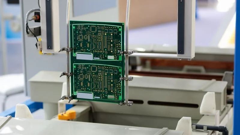
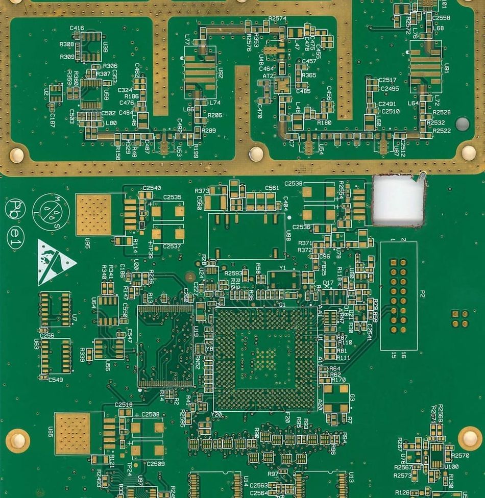
 Tracing the conductors of a multilayer printed circuit board
3.4. Immersion Tin
Immersion tin is a PCB surface finish that involves depositing a thin layer of tin onto exposed copper pads using an immersion process. This finish is lead-free, making it an environmentally friendly alternative to traditional tin-lead soldering processes. Immersion tin provides a uniform, flat surface, which is ideal for fine-pitch components and is compatible with various assembly processes, including surface mount technology (SMT), through-hole, and press-fit.
The immersion tin process involves dipping the PCB into a bath containing a tin salt solution, typically stannous sulfate or stannous fluoborate, which reacts with the copper surface to form a tin layer. The thickness of the deposited tin layer is typically between 0.8 to 1.2 µm, which provides a sufficient barrier against copper oxidation while ensuring good solderability.
One of the key advantages of immersion tin is its compatibility with lead-free soldering processes, as it can withstand the higher temperatures required for these methods. Additionally, the flat, uniform surface provided by the tin layer ensures that fine-pitch components can be accurately placed during assembly, reducing the risk of solder bridging or other defects.
Immersion tin also exhibits strong solder joint formation due to the intermetallic compounds (IMC) formed between tin and copper during the soldering process. These IMCs, such as Cu6Sn5 and Cu3Sn, improve the mechanical and thermal properties of the solder joint, contributing to the overall reliability of the assembled PCB.
3.5. Immersion Silver
Immersion silver is another popular PCB surface finish that involves depositing a thin layer of silver onto the exposed copper pads using a chemical immersion process. This finish offers several advantages, including excellent solderability, low contact resistance, and compatibility with lead-free soldering processes. Additionally, immersion silver provides a smooth, planar surface, which is suitable for fine-pitch components and high-frequency applications.
The immersion silver process consists of dipping the PCB into a silver salt solution, such as silver cyanide or silver sulfamate. The solution reacts with the copper surface to deposit a thin layer of silver, typically ranging from 0.12 to 0.4 µm in thickness. This silver layer protects the underlying copper from oxidation and provides a good surface for soldering.
One of the main benefits of immersion silver is its excellent solderability, which results from the strong intermetallic compounds (IMC) formed between the silver layer and the solder. The most common IMC formed during the soldering process is Ag3Sn, which exhibits high mechanical strength and thermal stability, contributing to the overall reliability and performance of the solder joint.
Immersion silver is also well-suited for high-frequency applications due to its low contact resistance and signal loss characteristics. The silver layer offers low surface roughness, which is particularly beneficial for high-speed signal transmission and helps minimize insertion loss and crosstalk.
3.6. ENEPIG (Electroless Nickel Electroless Palladium Immersion Gold)
ENEPIG is a multilayer surface finish for PCBs that consists of electroless nickel, electroless palladium, and immersion gold layers. This surface finish offers a combination of benefits from its constituent metals, such as excellent solderability, wire bondability, and corrosion resistance. ENEPIG is particularly suitable for applications requiring long-term reliability, mixed assembly technologies, and compatibility with various soldering and wire bonding processes.
The ENEPIG process involves the sequential deposition of nickel, palladium, and gold layers onto the exposed copper pads of a PCB. The electroless nickel layer, typically 3 to 5 µm thick, serves as a barrier between the copper and palladium layers, protecting the copper from oxidation and enhancing the overall corrosion resistance of the PCB. The electroless palladium layer, ranging from 0.05 to 0.15 µm in thickness, provides a stable surface for the subsequent immersion gold layer and improves the solder joint reliability.
The final immersion gold layer is thin, typically around 0.03 to 0.05 µm, and serves as a protective layer for the underlying palladium. This gold layer also provides excellent solderability and wire bondability, making ENEPIG suitable for a wide range of assembly processes, including lead-free soldering and gold wire bonding.
One of the main advantages of ENEPIG is its compatibility with multiple assembly technologies. The surface finish can accommodate both soldering and wire bonding processes, making it an ideal choice for mixed assembly applications or products requiring multiple interconnection methods.
ENEPIG also exhibits excellent solder joint reliability due to the formation of strong and stable intermetallic compounds (IMC) during the soldering process. In the case of ENEPIG, the most common IMC is (Ni,Pd)Sn, which has desirable mechanical and thermal properties that contribute to the overall performance and longevity of the solder joint.
4. Comparing PCB Surface Finishes
Each PCB surface finish has unique features that make it suitable for certain applications. Let's compare the common PCB surface finishes to better understand their differences:
4.1. Surface Finish Comparison Chart
To assist in understanding the differences between common PCB surface finishes, a comparison chart can be beneficial. This chart takes into account key attributes of each surface finish, including cost, solderability, corrosion resistance, shelf life, and compatibility with assembly processes.
HASL (Hot Air Solder Leveling)
Cost: Low
Solderability: Good
Corrosion Resistance: Moderate
Shelf Life: Moderate, typically 12 months
Assembly Compatibility: Suitable for conventional soldering processes
ENIG (Electroless Nickel Immersion Gold)
Cost: Moderate
Solderability: Excellent
Corrosion Resistance: Excellent
Shelf Life: Long, up to 24 months
Assembly Compatibility: Suitable for lead-free soldering and wire bonding
OSP (Organic Solderability Preservatives)
Cost: Low
Solderability: Good
Corrosion Resistance: Moderate
Shelf Life: Short, typically 6 months
Assembly Compatibility: Suitable for lead-free soldering
Immersion Tin
Cost: Moderate
Solderability: Excellent
Corrosion Resistance: Moderate
Shelf Life: Moderate, typically 12 months
Assembly Compatibility: Suitable for lead-free soldering
Immersion Silver
Cost: Moderate
Solderability: Excellent
Corrosion Resistance: Moderate
Shelf Life: Moderate, typically 12 months
Assembly Compatibility: Suitable for lead-free soldering
ENEPIG (Electroless Nickel Electroless Palladium Immersion Gold)
Cost: High
Solderability: Excellent
Corrosion Resistance: Excellent
Shelf Life: Long, up to 24 months
Assembly Compatibility: Suitable for lead-free soldering, wire bonding, and mixed assembly
Recommended Reading: HASL vs ENIG Surface Finishes: Understanding the difference (REDIRECT) (REDIRECT) (REDIRECT)
4.2. Best Practices for Selecting a Surface Finish
Selecting the appropriate surface finish for a PCB is a crucial step in the design and manufacturing process. The right finish can enhance the board's performance, reliability, and longevity, while an unsuitable finish can lead to potential issues such as corrosion, solderability problems, and increased cost. Here are some best practices for selecting a surface finish that meets the requirements of the specific application:
Assess the application requirements: The first step in selecting a surface finish is to carefully evaluate the requirements of the application. Consider factors such as the operating environment, temperature range, and mechanical stress that the PCB will be subjected to. Additionally, take into account the specific components that will be mounted on the board and their compatibility with different surface finishes.
Evaluate soldering processes: The soldering process used in the assembly of the PCB plays a significant role in determining the most suitable surface finish. For example, lead-free soldering processes may require different surface finishes than traditional leaded soldering. Review the soldering process and its compatibility with various finishes before making a decision.
Consider corrosion resistance: Corrosion resistance is an important factor in selecting a surface finish, particularly for PCBs that will be exposed to harsh environments or fluctuating temperatures. Evaluate the corrosion resistance of each surface finish and choose one that offers adequate protection for the specific application.
Examine shelf life: Shelf life refers to the period during which a PCB can be stored before its performance begins to degrade. Different surface finishes offer varying shelf lives, so it is essential to consider the storage and handling requirements of the PCBs when selecting a surface finish.
Analyze cost and complexity: The cost and complexity of applying a surface finish should be considered, as these factors can impact the overall project budget and timeline. While some finishes may offer superior performance, they may also require more intricate processes and increased costs. Assess the balance between cost, complexity, and performance when selecting a surface finish.
5. Surface Finish Standards
5.1. IPC Standards
IPC standards provide the guidelines and specifications for the design, manufacturing, and assembly of printed circuit boards. These standards ensure the quality, reliability, and consistency of PCBs and their surface finishes. Several key IPC standards relate to PCB surface finishes, including IPC-4552, IPC-4553, IPC-4554, and IPC-4556.
IPC-4552 is the standard for electroless nickel immersion gold (ENIG) surface finishes. This standard specifies the requirements for the thickness of the nickel and gold layers, as well as the acceptable appearance, solderability, and adhesion properties. The standard calls for a minimum thickness of 3 to 6 µin (0.076 to 0.152 µm) for the gold layer and a minimum thickness of 118 to 236 µin (3 to 6 µm) for the nickel layer.
IPC-4553 addresses the requirements for immersion silver surface finishes. This standard outlines the acceptable thickness range, appearance, and solderability of the silver layer on PCBs. According to IPC-4553, the immersion silver layer should have a thickness between 8 and 20 µin (0.2 to 0.5 µm).
IPC-4554 is the standard for electroless nickel electroless palladium immersion gold (ENEPIG) surface finishes. This standard provides guidelines for the thicknesses of the nickel, palladium, and gold layers, as well as the required appearance, solderability, and adhesion properties. IPC-4554 recommends a nickel layer thickness of 118 to 236 µin (3 to 6 µm), a palladium layer thickness of 4 to 20 µin (0.1 to 0.5 µm), and a gold layer thickness of 1 to 2 µin (0.025 to 0.051 µm).
IPC-4556 pertains to the electroless nickel immersion palladium gold (ENIPIG) surface finish. This standard specifies the thickness requirements for the nickel, palladium, and gold layers, as well as the acceptable appearance, solderability, and adhesion properties. IPC-4556 requires a nickel layer thickness of 118 to 236 µin (3 to 6 µm), a palladium layer thickness of 4 to 20 µin (0.1 to 0.5 µm), and a gold layer thickness of 1 to 2 µin (0.025 to 0.051 µm).
5.2. RoHS and REACH Compliance
RoHS and REACH are two significant environmental regulations that impact the electronics industry and PCB surface finishes. Both directives aim to restrict the use of hazardous substances in the production of electronic devices and components.
RoHS, which stands for Restriction of Hazardous Substances, is a European Union directive that limits the use of certain toxic substances in electrical and electronic equipment. RoHS restricts the use of six hazardous substances, including lead, mercury, cadmium, hexavalent chromium, polybrominated biphenyls (PBB), and polybrominated diphenyl ethers (PBDE). The RoHS directive has a direct impact on PCB surface finishes, as it requires the use of lead-free alternatives, such as ENIG, ENEPIG, and immersion silver.
REACH, or the Registration, Evaluation, Authorization, and Restriction of Chemicals, is another European Union regulation that affects the electronics industry. REACH aims to improve the protection of human health and the environment by controlling the production and use of chemicals. The regulation requires manufacturers and importers to register chemicals used in their products and ensure compliance with safety standards.
PCB surface finishes must comply with both RoHS and REACH regulations. Manufacturers need to ensure that the materials and processes used in their surface finishes are in line with these directives. To maintain compliance, it is essential to select surface finishes that do not contain restricted substances or have substitutes that meet the RoHS and REACH requirements. Additionally, manufacturers must maintain proper documentation and undergo regular audits to verify compliance.
6. Advanced PCB Surface Finish Technologies
As the electronics industry continues to evolve, advanced PCB surface finish technologies are emerging to meet the changing demands of new applications. Here are a few innovative surface finish technologies that are gaining traction:
6.1. Nano-Coatings
Nano-coatings are an emerging technology in the field of PCB surface finishes, offering enhanced properties for specific applications. These coatings, composed of nanoscale particles, have unique characteristics due to their small size and high surface area. Nano-coatings can be applied to various base materials, including metals, ceramics, and polymers, to enhance their properties and performance.
One of the key benefits of nano-coatings is their ability to provide a barrier against moisture, oxidation, and corrosion. This is particularly important for PCBs used in harsh environments or exposed to chemicals. Nano-coatings can also improve the electrical conductivity of the underlying surface, which is critical for high-speed and high-frequency applications. Furthermore, these coatings offer increased thermal stability and resistance to wear, which can extend the life of PCBs.
One example of nano-coatings is graphene-based coatings. Graphene, a single layer of carbon atoms arranged in a hexagonal lattice, has exceptional electrical, thermal, and mechanical properties. Graphene coatings can enhance the performance of PCB surface finishes by providing excellent conductivity, thermal stability, and wear resistance. Additionally, graphene coatings offer a high degree of flexibility, making them suitable for use with flexible PCBs.
Another example is nano-silver coatings, which consist of silver nanoparticles suspended in a matrix. These coatings provide excellent electrical conductivity and can be used as an alternative to traditional silver-based finishes. Nano-silver coatings can be applied using various methods, including electroless deposition, which allows for uniform coverage and thickness control.
6.2. Hybrid Surface Finishes
Hybrid surface finishes represent a combination of two or more surface finish technologies to achieve improved performance, reliability, and durability in PCB applications. By utilizing the advantages of multiple finishes, hybrid solutions can provide tailored properties to meet specific design requirements or overcome limitations associated with single finish types.
One example of a hybrid surface finish is the combination of electroless nickel immersion gold (ENIG) and electroless nickel electroless palladium immersion gold (ENEPIG). This approach takes advantage of the excellent solderability and wire bondability provided by ENEPIG, while also benefiting from the good electrical conductivity and corrosion resistance of ENIG. In this case, the hybrid finish consists of a thin layer of palladium between the nickel and gold layers, which helps to prevent nickel corrosion and improve the overall performance of the finish.
Another example of a hybrid surface finish is the integration of organic solderability preservatives (OSPs) with immersion silver or immersion tin. This combination can enhance the solderability and shelf life of the OSP finish while preserving the low-cost advantages of immersion silver or tin. By incorporating a thin layer of OSP over the metallic finish, the hybrid solution can provide improved protection against oxidation and reduce the likelihood of solder joint failures.
Hybrid surface finishes can also involve the combination of nano-coatings with traditional finishes. For instance, applying a graphene-based nano-coating over an immersion silver finish can improve electrical conductivity, thermal stability, and wear resistance. At the same time, the nano-coating serves as a barrier against moisture and corrosion, extending the life of the PCB.
The development of hybrid surface finishes is driven by the need for optimized performance in a diverse range of applications. These solutions enable designers to address specific challenges, such as achieving high-frequency performance, enhancing corrosion resistance, or improving solderability. As the electronics industry continues to evolve and demand more complex and high-performance PCBs, the use of hybrid surface finishes is expected to increase, offering tailored solutions for various application requirements.
7. PCB Surface Finish Handling and Storage
Proper handling and storage of PCBs with different surface finishes are crucial to maintain their integrity and performance. Here are some general guidelines:
7.1. Handling Guidelines
Proper handling of PCBs with different surface finishes is critical to ensure their performance, reliability, and longevity. Adhering to specific handling guidelines can help prevent contamination, oxidation, and physical damage that may compromise the functionality of the PCB.
One of the essential handling guidelines is to always wear gloves when handling PCBs. Human skin contains oils and salts that can contaminate the surface finish, leading to oxidation and reduced solderability. Gloves made of non-contaminating materials, such as nitrile or lint-free cotton, are recommended to prevent contamination transfer.
Another important handling guideline is to avoid touching the surface finish directly, especially the conductive areas, as this can cause damage or contamination. If it is necessary to handle a PCB directly, only touch the edges or use specialized tools, such as tweezers or vacuum pick-up systems, to minimize contact with the surface finish.
When stacking PCBs for storage or transportation, it is crucial to use spacers or separators to prevent direct contact between the boards. This prevents scratches or other physical damage to the surface finish. The use of antistatic materials for separators is also recommended to avoid potential electrostatic discharge (ESD) damage to sensitive components.
Proper grounding is essential when working with PCBs to prevent ESD damage. Personnel should wear ESD wrist straps connected to a common ground point, and workstations should have grounded ESD mats. Also, ensure that all tools and equipment used for handling PCBs are ESD-safe.
7.2. Storage Considerations
Proper storage of PCBs with surface finishes is critical to maintain their quality and performance. Storage conditions play a significant role in preventing oxidation, contamination, and other forms of degradation that can impact the functionality of the PCB.
Temperature control is a crucial aspect of PCB storage. High temperatures can accelerate oxidation processes and cause solder materials to degrade. It is generally recommended to store PCBs in a temperature-controlled environment with a range of 20-25°C (68-77°F). However, specific temperature requirements may vary depending on the type of surface finish used.
Humidity control is another essential factor in PCB storage. High humidity levels can cause corrosion and oxidation of the surface finish, while low humidity levels can increase the risk of electrostatic discharge (ESD) damage. A relative humidity of 40-60% is typically recommended for PCB storage. However, some surface finishes may have more specific humidity requirements. To maintain the recommended humidity levels, consider using dehumidifiers or humidifiers in the storage area.
Proper packaging is essential to protect PCBs during storage. Antistatic bags, moisture barrier bags, or sealed containers should be used to prevent the ingress of moisture and to shield the PCBs from electrostatic discharge. Desiccant packs can be added to the packaging to help maintain low humidity levels inside.
Light exposure should also be considered, as some surface finishes may be sensitive to ultraviolet (UV) radiation. Prolonged exposure to UV light can cause discoloration or degradation of certain finishes. To mitigate this risk, store PCBs in opaque containers or in a location that limits direct exposure to sunlight or other UV light sources.
8. Conclusion
In conclusion, PCB surface finishes play a critical role in the performance, reliability, and longevity of electronic devices. Understanding the various surface finishes available, their properties, and how they impact PCB functionality is essential in selecting the best option for a specific application. Proper handling and storage of PCBs are also crucial to preserving the quality of the surface finish and ensuring optimal performance throughout the product's lifecycle. With continued advancements in surface finish technologies, such as nano-coatings and hybrid finishes, the electronics industry will continue to benefit from enhanced performance and durability of PCBs.
9. Frequently Asked Questions (FAQs)
What factors should be considered when selecting a PCB surface finish?
When selecting a PCB surface finish, consider factors such as solderability, signal integrity, durability, environmental impact, and cost. The specific requirements of your application and the operating environment should guide your selection process.What are the most common PCB surface finishes?
The most common PCB surface finishes include Hot Air Solder Leveling (HASL), Electroless Nickel Immersion Gold (ENIG), Immersion Silver, Immersion Tin, and Organic Solderability Preservative (OSP).What is the difference between RoHS and REACH compliance?
RoHS (Restriction of Hazardous Substances) is a European directive that restricts the use of specific hazardous materials in electrical and electronic devices. REACH (Registration, Evaluation, Authorisation, and Restriction of Chemicals) is another European regulation that aims to improve the protection of human health and the environment from chemical risks.How can I ensure proper handling and storage of PCBs with surface finishes?
Proper handling and storage of PCBs involve temperature and humidity control, appropriate packaging, minimizing exposure to UV light, and adhering to the manufacturer's guidelines for storage and shelf life.What are some emerging surface finish technologies?
Emerging surface finish technologies include nano-coatings, which can enhance the performance and durability of PCBs, and hybrid surface finishes that combine the benefits of multiple finishes to address specific application requirements.
References:
https://www.protoexpress.com/blog/surface-finish-pcb-manufacturing/
in this article
1. Introduction1. PCB Surface Finish: Definition and Purpose2. Factors to Consider When Choosing a PCB Surface Finish3. Common PCB Surface Finishes4. Comparing PCB Surface Finishes5. Surface Finish Standards6. Advanced PCB Surface Finish Technologies7. PCB Surface Finish Handling and Storage8. Conclusion9. Frequently Asked Questions (FAQs)11. References: