Mastering PCB Reverse Engineering: A Comprehensive Guide
Mastering PCB Reverse Engineering: Techniques, Tools, and Best Practices for Success in Electronics

13 Oct, 2023. 24 minutes read
Mastering PCB Reverse Engineering: Techniques, Tools, and Best Practices for Success in Electronics
No time now? Save for later.
We only use your email to send this link. Privacy Policy.
Introduction
PCB reverse engineering stands as a pivotal and intricate process within the dynamics of the electronics industry. It encompasses the meticulous analysis and meticulous reproduction of an existing printed circuit board (PCB), with the ultimate goal of crafting a new design that matches its functionality. This process serves as a linchpin for a myriad of purposes, including the meticulous replacement of outdated components, the safeguard of valuable intellectual property, and the thorough execution of competitive analysis.
In this article, you will delve into the world of PCB reverse engineering, exploring its applications, processes, techniques, tools, challenges, and best practices. you will also get to know the importance of following best practices and adhering to ethical and legal guidelines when reverse engineering PCBs. By the end of this article, you will have a comprehensive understanding of PCB reverse engineering and its role in the electronics industry.
1. What is PCB Reverse Engineering
PCB reverse engineering is the process of analyzing an existing printed circuit board (PCB) and reproducing its design to create a new, functionally equivalent version. This process involves several steps, including the extraction of schematic diagrams, reconstruction of the PCB layout, and creation of a bill of materials (BOM).
Key Reasons for PCB Reverse Engineering
Engineers undertake PCB reverse engineering for several reasons. One is the need to replace obsolete components with suitable alternatives, which often involves precise calculations using formulas like:
C= I/ΔV
Where:
C = Capacitance (in Farads)
I = Current (in Amperes)
ΔV = Voltage Ripple (in Volts)
Another motive is gaining insights into a competitor's product for competitive analysis. Advanced techniques like X-ray tomography may be used to unveil concealed design details. Additionally, it's a strategic tool for protecting intellectual property.
Exploring PCB Reverse Engineering
This article provides an overview of PCB reverse engineering, including its applications, processes, techniques, and tools. It also addresses the associated challenges and best practices. By the end, you'll understand its significance in the electronics industry and its role in innovation and IP protection.
Recommended Reading: What Is Reverse Engineering?
2. Applications of PCB Reverse Engineering
PCB reverse engineering has a wide range of applications in the electronics industry, each offering unique technical challenges and opportunities. In this section, we will discuss each of these applications in detail, providing practical examples, technical insights, formulas and derivations where relevant.
Obsolete Component Replacement
One of the primary applications of PCB reverse engineering is the replacement of obsolete components. As electronic components age and become outdated, they may no longer be available for purchase or may become prohibitively expensive to source. In these cases, engineers must find suitable replacement components that can maintain the functionality of the original design.
Practical Example: Imagine a vintage audio amplifier that has been a beloved piece of equipment for years. However, one day, a critical transistor becomes obsolete, and finding an exact replacement becomes impossible. PCB reverse engineering comes to the rescue.
Technical Insights: Engineers employ formulas such as Ohm's Law (V = IR) to calculate current (I), voltage (V), and resistance (R). When selecting replacement components, they assess parameters like the transistor's gain (hfe) and power dissipation (Pd) to ensure they match the original.
Additional Applications: Beyond component replacements, PCB reverse engineering aids in redesigning circuits for improved efficiency, enhancing thermal management, and adapting to evolving industry standards.
Intellectual Property Protection
Another important application of PCB reverse engineering is the protection of intellectual property (IP). In the electronics industry, companies invest significant resources in research and development to create innovative products and technologies. Protecting these innovations from unauthorized copying or reverse engineering by competitors is crucial to maintaining a competitive edge and ensuring the long-term success of the company.
PCB reverse engineering can play a vital role in IP protection by helping companies identify potential patent infringements or trade secret violations. By reverse engineering their own products or those of competitors, engineers can analyze the design and functionality of the PCBs to determine if any proprietary technologies or patented components have been copied or misused.
Practical Example: A tech company has developed an innovative fitness tracker with a unique sensor fusion algorithm that accurately measures user activity. To safeguard this breakthrough, they use PCB reverse engineering to monitor the market for unauthorized clones.
Technical Insights: Engineers perform signal analysis and statistical techniques to reverse engineer algorithms and sensor fusion methods. They apply mathematical derivations and simulations to validate the uniqueness of their technology.
Additional Applications: PCB reverse engineering extends to identifying IP infringements in integrated circuits (ICs), firmware, and embedded systems.
Competitive Analysis
PCB reverse engineering can also be used as a tool for competitive analysis, allowing companies to gain insights into the design and functionality of their competitors' products. By understanding the strengths and weaknesses of competing products, companies can identify opportunities for improvement in their own designs and develop strategies to differentiate themselves in the market.
The process of reverse engineering a competitor's PCB involves analyzing the schematic, layout, and bill of materials to determine the design choices and component selections made by the competitor. This information can provide valuable insights into the competitor's design philosophy, manufacturing processes, and cost structure.
Practical Example: An electronics manufacturer wants to understand how a competitor's smartphone achieves superior battery life. They reverse engineer the device's PCB to uncover power management strategies and optimize their designs.
Technical Insights: Engineers delve into power management circuitry, employing energy efficiency equations like:
Efficiency (%) = Pout/Pin × 100%
Where:
Pout = Output Power
Pin = Input Power
They analyze signal integrity through transmission line equations, ensuring high-speed data transfer and minimal signal degradation.
Additional Applications: PCB reverse engineering can reveal competitors' RF (Radio Frequency) design choices, enabling better RF circuit designs for wireless devices. It's also applied in reverse engineering protocols for communication interfaces.
Design Validation and Troubleshooting
PCB reverse engineering plays a pivotal role in design validation and troubleshooting, offering engineers a valuable toolkit for ensuring the functionality and reliability of electronic products. Throughout the product development lifecycle, from prototyping to mass production, challenges and issues inevitably arise. This application of PCB reverse engineering helps identify and address these challenges effectively.
Practical Example: In the development of complex electronic devices, such as smartphones or IoT devices, ensuring consistent performance is paramount. However, intermittent connectivity problems may emerge during testing. By reverse engineering the PCBs of affected units and conducting detailed signal analysis, engineers can trace the root causes of these issues. For instance, they may uncover signal interference, impedance mismatches, or faulty components that lead to signal degradation.
Technical Insights: PCB reverse engineering for design validation involves a comprehensive examination of the board's electrical characteristics. Engineers employ a range of technical tools and methodologies, including:
- Signal Processing Techniques: Fourier analysis and spectral analysis help identify frequency-domain characteristics and noise sources affecting signal integrity.
- Impedance Matching Calculations: Engineers calculate transmission line impedances, ensuring proper signal propagation and minimizing signal reflection.
- Noise Margin Analysis: Engineers assess noise margins to ensure that digital signals remain within their defined voltage thresholds, reducing the risk of data corruption.
- Thermal Analysis: In devices sensitive to temperature, thermal analysis tools and calculations are employed to evaluate heat dissipation and ensure components stay within their specified operating temperature ranges.
Additional Applications: Beyond design validation and troubleshooting, PCB reverse engineering supports iterative design improvements. Engineers can identify opportunities to optimize the design for factors like power efficiency, thermal management, and cost reduction. Furthermore, the insights gained from reverse engineering feed into the refinement of future product iterations, ensuring that electronic devices evolve to meet the demands of an ever-changing market.
Quality Control and PCB Manufacturing Optimization
Within the domain of PCB reverse engineering, this application combines two critical facets: quality control and manufacturing optimization. Quality Control involves meticulous scrutiny of each manufacturing stage, leveraging advanced techniques like Automated Optical Inspection (AOI), X-ray inspection, and In-Circuit Testing (ICT) to detect defects such as soldering issues or component misalignment, ensuring PCBs meet rigorous quality standards. Simultaneously, Manufacturing Optimization entails enhancing the overall manufacturing process. Engineers employ technical strategies like process simulation for workflow refinement, materials analysis for waste reduction and cost-effectiveness, and Statistical Process Control (SPC) techniques for real-time process monitoring. This integration of technical approaches leads to efficient, cost-effective, and eco-friendly PCB manufacturing, ensuring the consistent production of high-quality boards.
Practical Example: A PCB assembly line experiences high rejection rates due to soldering defects. Reverse engineering the PCBs of rejected units helps pinpoint the root causes, leading to process optimizations.
Technical Insights: Engineers employ statistical process control (SPC) techniques, such as control charts and process capability analysis, to monitor and enhance manufacturing processes.
Additional Applications: PCB reverse engineering enhances yield optimization, reducing waste and ensuring high-quality products.
In summary, PCB reverse engineering can provide valuable insights into competitor products, allowing companies to identify opportunities for improvement and differentiation in their own designs. By understanding the design choices and component selections made by competitors, companies can make informed decisions about their own product development efforts and maintain a competitive edge in the market.
Recommended Reading: How to Get Started with Product Reverse Engineering?
3. PCB Reverse Engineering Process
The PCB reverse engineering is an intricate journey comprising several meticulously executed phases: preparation, schematic generation, PCB layout reconstruction, and bill of materials (BOM) creation. Each phase is a linchpin, vital for the accuracy and success of the overall reverse engineering endeavor. In this section, we'll navigate through each phase, immersing ourselves in the technical depths while also unveiling the challenges and advanced techniques that underpin the process.
Preparation
Proper preparation is essential for a successful PCB reverse engineering process. It involves a strategic orchestration of essential tools and precise PCB conditioning for in-depth analysis. The arsenal of tools and equipment for PCB reverse engineering encompasses:
- Optical inspection tools: These include high-resolution microscopes and cameras, equipped with features like digital zoom and adjustable lighting for meticulous visual scrutiny of the PCB. The objective is to unveil the nuances of the PCB's layout.
- X-ray inspection equipment: Utilized for non-destructive analysis, X-ray machines peer into the inner layers and concealed vias, unveiling the board's hidden intricacies. Advanced X-ray tomography techniques are employed for precise 3D reconstructions of the PCB.
- Electrical testing equipment: Multimeters, oscilloscopes, and flying probes are employed for comprehensive electrical characterization. These instruments verify not only the overall functionality of the PCB but also the performance of individual components and their interconnections.
- Software tools: Specialized EDA (Electronic Design Automation) software, such as Altium Designer and KiCad, augments the analysis process by enabling precise schematic generation, PCB layout reconstruction, and BOM creation.
Preparing the PCB for reverse engineering may involve several tasks, including:
- Exhaustive cleaning: The first task is to cleanse the PCB thoroughly, expelling contaminants such as dirt, dust, and particulate matter that could obscure critical details during subsequent inspection and analysis.
- Strategic coating removal: When warranted, protective or conformal coatings are methodically stripped away, laying bare the underlying components and intricate traces for scrutiny.
- De-soldering and component extraction: As necessity dictates, a delicate de-soldering process is executed, extracting components from the PCB. This step is instrumental in enabling an in-depth examination and analysis of the underlying traces and intricate connections.
The significance of this phase cannot be overstated; it forms the robust foundation upon which the entire reverse engineering process stands. Proper preparation, akin to the calibration of scientific instruments, serves to minimize the potential for errors and inaccuracies, ensuring the subsequent stages of reverse engineering yield reliable and accurate results.
Schematic Generation
Schematic generation stands as a linchpin within the intricate PCB reverse engineering process, holding the key to unraveling the secrets concealed within the printed circuit board (PCB). It is the art of meticulously crafting a detailed representation of the labyrinthine electrical connections and the intricate tapestry of components that comprise the PCB. This schematic, akin to a technical blueprint, not only elucidates the intricate interplay of circuitry but also lays the foundational groundwork for the subsequent reconstruction of the PCB layout.
The process of transmuting a physical PCB into a comprehensive schematic typically unfolds in a sequence of steps that are both intricate and demanding:
- Tracing connections: A fundamental first stride involves the meticulous tracing of connections between individual components on the PCB. This is achieved through a symphony of optical inspection tools, equipped with high magnification and precision, and electrical testing equipment, including oscilloscopes and multimeters. The complexity of this task escalates exponentially when dealing with multi-layer PCBs that harbor dense routing and a profusion of components.
- Identifying components: Engineers take on the role of forensic investigators, scrutinizing each component on the PCB with utmost precision. This involves deciphering not just their physical attributes but diving deeper into their intrinsic characteristics, including type, value, and function. This exhaustive component identification is the cornerstone upon which an accurate schematic is erected, and it is pivotal in ensuring the flawless functionality of the reverse-engineered PCB.
- Creating the schematic: Armed with a wealth of meticulously gathered data, engineers proceed to craft a digital representation of the PCB's intricate tapestry. Specialized software tools, endowed with the ability to translate the tangible into the digital realm, are wielded with dexterity. The resultant schematic is a masterstroke of engineering artistry, replete with component symbols, reference designators, and intricate connection points.
The art of schematic generation is not without its fair share of challenges and requires the application of ingenious techniques:
- Navigating Complexity: Tracing connections on densely populated PCBs is akin to deciphering an intricate maze, and utmost care must be taken to ensure that each connection is faithfully transcribed. The risk of introducing errors looms large, necessitating a surgeon's precision.
- Exploring the Hidden: In the quest for an exhaustive schematic, engineers are often compelled to explore the hidden recesses of the PCB. This includes delving into internal layers and uncovering concealed vias, a task that is made feasible through the deployment of advanced X-ray inspection equipment, utilizing X-ray tomography techniques.
Assisting engineers in this endeavor are a plethora of software tools. Prominent among them are Electronic Design Automation (EDA) tools like Altium Designer, Cadence OrCAD, and Mentor Graphics PADS. These EDA tools offer a multifaceted suite of capabilities that include automated connection tracing, expansive component libraries, and vigilant error checking mechanisms. These features not only streamline the schematic generation process but also augment the accuracy and reliability of the resulting schematic.
In summary, schematic generation is the alchemical process through which a tangible PCB is transformed into a digital representation, encapsulating the essence of its intricate electrical connections and components. It is a journey fraught with complexity and intricacy, where precision and advanced technology converge to unlock the secrets hidden within the heart of the PCB.
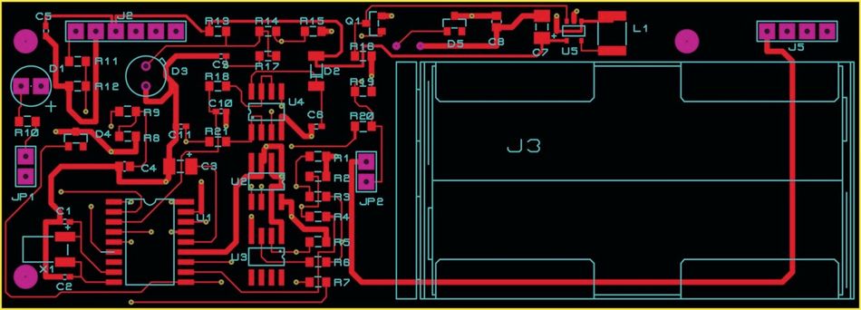
PCB Layout Reconstruction
Once the schematic has been generated, the next step in the PCB reverse engineering process is to reconstruct the PCB Layout. The layout is a critical aspect of PCB design, as it determines the physical arrangement of components, traces, and vias on the board. A well-designed layout can improve signal integrity, reduce electromagnetic interference, and optimize thermal performance.
Reconstructing the PCB layout from a schematic involves the following steps:
- Component placement: Engineers embark on a meticulous journey to ascertain the optimal positioning of electronic components on the PCB. This task is multifaceted, entailing a deep consideration of factors such as signal integrity, thermal performance, and manufacturability. A detailed analysis of the original PCB is imperative, shedding light on the logical underpinnings of component placement. Engineers may find it necessary to make nuanced adjustments to accommodate replacement components or incorporate design enhancements, all while adhering to the principles of through-hole and surface-mount device (SMD) integration.
- Routing: Subsequent to the judicious placement of components, engineers undertake the intricate process of routing electrical connections with utmost precision. The schematic acts as a guiding light in this endeavor, delineating the path for traces and vias that establish vital connections. This phase demands a meticulous approach to minimize potential challenges such as signal interference, crosstalk, and other electromagnetic considerations. Adherence to design rules and manufacturing constraints is non-negotiable; parameters like trace width, spacing, and via dimensions must align seamlessly to ensure the PCB's reliable and efficient fabrication.
- Design verification: At the conclusion of the layout reconstruction, engineers engage in rigorous design verification processes. The objective is to validate that the layout faithfully mirrors the schematic and meticulously adheres to all design specifications. This verification process encompasses a spectrum of activities, from the execution of sophisticated simulations that assess electrical performance to comprehensive design rule checks ensuring that the layout meets or exceeds industry standards. Additionally, thermal analysis becomes paramount, assuring that the PCB will function with absolute precision even under extreme conditions.
Reconstructing the PCB layout can be a complex and time-consuming process, particularly for multi-layer boards with dense routing and numerous components. Engineers must carefully consider factors such as signal integrity, thermal performance, and manufacturability when creating the layout, ensuring that the reverse-engineered PCB will function as intended.
The toolkit available to engineers is rich and versatile, with a plethora of software tools designed explicitly for PCB layout reconstruction. Renowned electronic design automation (EDA) tools like Altium Designer, Cadence Allegro, and Mentor Graphics PADS lead the way, providing a wide array of functionalities encompassing automated routing, stringent design rule validation, and robust simulation capabilities.
In harnessing these powerful tools and adhering diligently to the detailed steps, engineers navigate the intricate landscape of PCB layout reconstruction. They ensure that the resulting layout is not merely a faithful representation of the original but an optimized blueprint for superior PCB performance. Thus, the reverse-engineered PCB evolves into a technological masterpiece that adheres to the highest industry standards and leverages cutting-edge capabilities.
Bill of Materials (BOM) Creation
The final step in the PCB reverse engineering process is the creation of a bill of materials (BOM). The BOM is a comprehensive list of all the components used in the PCB, including their specifications, quantities, and reference designators. An accurate BOM is essential for ensuring the correct components are sourced and assembled during the fabrication process, as well as for maintaining inventory and managing component obsolescence.
Creating a BOM during PCB reverse engineering involves the following tasks:
- Component identification: Engineers embark on a rigorous process of meticulously identifying each constituent element adorning the PCB. This identification involves an intricate dissection of each component, unraveling its type, value, and function. The meticulously gathered component data forms the bedrock upon which the accurate BOM is meticulously structured, ultimately culminating in the seamless operation of the reverse-engineered PCB.
The process of identifying electronic components can be succinctly represented by Ohm's Law, a fundamental equation in electronics:
V=I×R
Here, V represents voltage, I symbolizes current, and R denotes resistance. Engineers employ various techniques, including multimeters, to measure these values, allowing for the precise identification and cataloging of components.
- Reference designator assignment: Each component nestling on the PCB must be attributed a unique reference designator. These designators serve as unequivocal identifiers that thread their way through the schematic, layout, and BOM. The format of reference designators typically conforms to a standardized nomenclature, exemplified by designations such as "R1" denoting the first resistor and "C1" signifying the first capacitor.
- Component sourcing information: A pivotal dimension of the BOM lies in the inclusion of comprehensive sourcing information. Beyond mere component specifications, the BOM should incorporate sourcing specifics, encompassing manufacturer part numbers and meticulously curated lists of approved vendors. This repository of information emerges as an indispensable resource, ensuring that the correct components are judiciously procured during the fabrication phase. It also acts as a bulwark against potential pitfalls associated with counterfeit or substandard components.
To calculate the total cost of components, the engineers employ a simple equation:
Total Cost=∑ (Quantity × Unit Cost)
Where "Quantity" represents the number of each component required, and "Unit Cost" is the cost per unit. This equation ensures accurate cost estimates, vital for budgeting and procurement.
Several software tools are available to assist with BOM creation, including popular electronic design automation (EDA) tools like Altium Designer, Cadence OrCAD, and Mentor Graphics PADS. These tools offer features such as automated BOM generation, component library management, and supplier integration, which can help streamline the BOM creation process and improve the accuracy of the resulting BOM.
In summary, creating a comprehensive and accurate BOM is a critical step in the PCB reverse engineering process, ensuring that the correct components are sourced and assembled during fabrication. By carefully identifying components, assigning reference designators, and providing sourcing information, engineers can create a BOM that supports the successful fabrication and assembly of the reverse-engineered PCB.
Recommended Reading: Components of a PCB: A Comprehensive Guide
4. Techniques and Tools for PCB Reverse Engineering
The realm of PCB reverse engineering relies heavily on a repertoire of meticulously crafted techniques and an arsenal of cutting-edge tools. These methodologies and instruments are the keystones upon which tasks like component identification, connection tracing, and schematic generation rest. In this section, we delve into a comprehensive exploration of some of the most extensively employed techniques and tools, encompassing optical inspection, X-ray analysis, electrical testing, and software utilities.
Optical Inspection
Optical inspection stands as a cornerstone in the domain of PCB reverse engineering, facilitating a visual pilgrimage through the intricate landscape of the PCB and its components. This journey is quintessential for a multitude of tasks, ranging from tracing connections to identifying components, and ultimately, verifying the precision of the schematic and layout.
Optical inspection tools used in PCB reverse engineering include:
- Microscopes: Stereo microscopes and their digital counterparts reign supreme as stalwart companions in magnifying and scrutinizing minuscule components, traces, and vias adorning the PCB. These optical marvels offer a range of magnification options, spanning from 10x to well over 100x, empowering engineers to explore the most diminutive intricacies on the board.
- High-resolution cameras: High-resolution cameras emerge as virtuosos in capturing intricate PCB imagery, subject to subsequent analysis via image processing software. These cameras boast resolutions scaling up to several megapixels, conferring the level of detail requisite for precise reverse engineering.
- Automated optical inspection (AOI) systems: While predominantly harnessed for quality control in PCB manufacturing, AOI systems wield potential in the realm of reverse engineering. These specialized contrivances orchestrate a symphony of cameras, lighting arrays, and image processing algorithms to meticulously scrutinize PCBs for anomalies or incongruities. This serves as an expeditious means of tracing connections and identifying components with unwavering precision.
Optical inspection techniques used in PCB reverse engineering include:
- Visual examination: Visual scrutiny conducted through microscopes and high-resolution cameras empowers engineers to explore the PCB's intricate tapestry. This exercise encompasses the identification of components, tracing of connections, and validation of the schematic and layout's accuracy.
- Image processing: Leveraging the prowess of image processing software, engineers analyze the troves of PCB images they capture. This software extracts invaluable insights, delineating component outlines, trace pathways, and via locations. Such data proves instrumental in expediting schematic generation and layout reconstruction.
By harnessing the prowess of optical inspection techniques and tools, engineers embarking on the odyssey of PCB reverse engineering pave the path towards accuracy and efficiency in their endeavors.
X-ray Inspection
X-ray inspection stands as a pivotal technique in the realm of PCB reverse engineering, serving as the X-ray vision into the heart of a PCB's concealed intricacies. This method plays an indispensable role in uncovering features that elude visual inspection alone. By harnessing the power of X-ray, engineers can peer through the layers of the PCB, delving deep into its internal structures, including enigmatic components like buried vias and inner layers. These elements are the linchpin for comprehending the holistic design of the PCB.
X-ray inspection equipment:
- X-ray machines: At the heart of this technique lie X-ray machines, which emit controlled X-rays that penetrate the PCB. These rays unveil the previously hidden features and structures within. It's noteworthy that X-ray machines used for PCB inspection operate at lower energy levels compared to their medical imaging counterparts. This not only ensures the safety of the operator but also minimizes the risk of damage to the PCB.
- X-ray detectors: Serving as the eyes of this process, X-ray detectors capture the X-rays as they traverse the PCB. Subsequently, these detectors convert these X-rays into high-resolution digital images. The quality and resolution of these detectors are instrumental in obtaining detailed images of the PCB's internal structures.
- X-ray inspection software: The third pillar of X-ray inspection is specialized software. This software plays a pivotal role in dissecting and analyzing the captured X-ray images. It extracts critical information such as layer stack-up, trace routing, and via locations. Furthermore, this software often boasts features such as image enhancement, measurement tools, and layer separation, which can help engineers better understand the PCB's internal structures.
X-ray inspection techniques:
- Layer separation: Engineers leverage X-ray inspection software to perform a meticulous dissection of multi-layer PCBs. This dissection enables the isolation of individual layers for in-depth, independent analysis. The technique proves exceptionally beneficial when tracing connections and identifying components residing on internal layers that remain elusive through optical inspection alone.
- Buried via analysis: Buried vias, those enigmatic connections concealed within the inner sanctum of a PCB without extending to the outer layers, are unveiled through X-ray inspection. This analysis not only reveals the location but also the intricate connectivity of these concealed vias. Such revelations offer invaluable insights, serving as the bedrock for reconstructing the PCB layout
- Internal trace routing: The third technique encompassed by X-ray inspection centers on tracing the labyrinthine routes of internal traces. These hidden pathways remain elusive to optical inspection but are pivotal for a comprehensive understanding of the PCB's design. It is imperative to ensure the accuracy of the reconstructed layout.
By deploying X-ray inspection techniques and wielding these sophisticated tools, engineers embark on a journey that allows them to penetrate the PCB's enigmatic inner structures. This results in elevated accuracy and a comprehensive understanding, leading to superior outcomes in the realm of reverse engineering. Moreover, to complement these techniques and tools, it is essential to incorporate the use of a netlist, which serves as a valuable guide in deciphering the connections within the PCB. Additionally, during the reverse engineering process, capturing the PCB's details can involve working with various file formats such as bitmap images and Gerber files. To facilitate the process, software applications like Inkscape and Autotrace can be implemented, allowing for the conversion of images into vector graphics. This transition from bitmap images to vector graphics simplifies the task of recreating intricate PCB schematics.
In a collaborative environment, where the pursuit of knowledge is open-source, engineers often come together to share their expertise and insights, creating a supportive ecosystem for reverse engineering services. As they navigate the PCB's design, they explore every side of the board and scrutinize the intricacies of the sides of the PCB. Notably, the top layer is meticulously examined, as it often holds critical information.
In summary, employing X-ray inspection techniques, advanced software tools, and integrating critical terminologies and open-source collaboration, engineers execute a comprehensive exploration of the PCB's hidden mysteries, thereby ensuring the accuracy and integrity of the reverse engineering process.
Electrical Testing
Electrical testing is an essential technique in PCB reverse engineering, as it helps engineers verify the functionality of the PCB and its components. By performing electrical tests, engineers can ensure that the reconstructed schematic and layout accurately represent the original PCB and that the reverse-engineered PCB will function as intended.
Some common electrical testing tools used in PCB reverse engineering include:
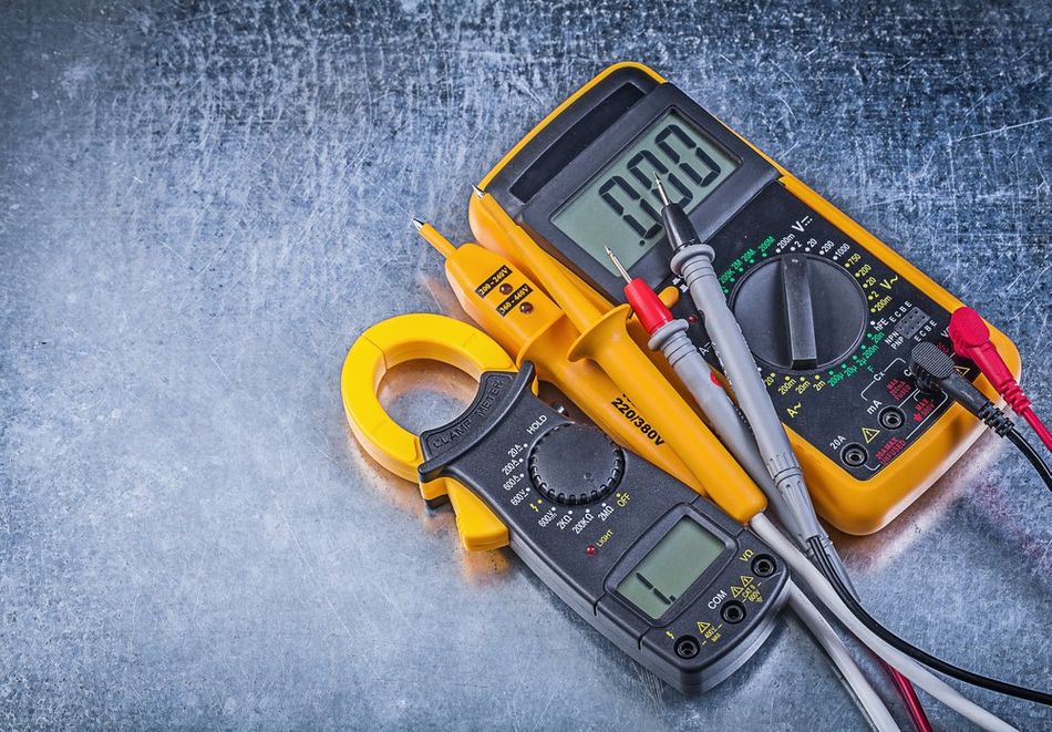
- Multimeters: Multimeters are versatile instruments capable of measuring voltage (V), current (I), resistance (R), and other electrical parameters. Engineers rely on them extensively in PCB reverse engineering to verify component specifications, trace continuity, and identify short circuits or open connections. A typical multimeter display is shown below:Digital clamp meter electric tester multimeter on metallic background.
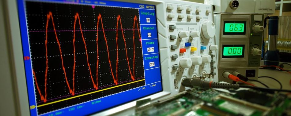
- Oscilloscopes: Oscilloscopes serve as invaluable tools for visualizing and analyzing electrical signals across the time domain. Their utility extends to examining analog circuit behaviors like those of power supplies and amplifiers, as well as troubleshooting signal integrity concerns in high-speed digital circuits. A sample oscilloscope waveform is depicted below:Measurement of a waveform with an oscilloscope
- Logic analyzers: Logic analyzers are used to capture and analyze digital signals, providing insight into the timing and state of digital circuits. They can be especially helpful for debugging complex digital systems, such as microcontrollers and FPGA-based designs.
Electrical testing techniques used in PCB reverse engineering include:
- Continuity testing: Engineers utilize multimeters for continuity testing, ensuring the integrity of electrical connections between components and detecting short circuits or open circuits. This procedure is pivotal for guaranteeing the precision of the reconstructed schematic and layout.
- Component testing: Engineers can use multimeters, oscilloscopes, and other testing equipment to verify the values and functionality of components on the PCB. This testing helps ensure that the correct components are identified and included in the BOM.
- Signal integrity testing: Oscilloscopes and logic analyzers come to the fore in examining electrical signal behaviors on the PCB. This testing pinpoints issues such as crosstalk, reflections, and electromagnetic interference, delivering crucial insights into the performance of the original PCB and aiding enhancements in the reverse-engineered design.
By proficiently implementing electrical testing techniques and leveraging the appropriate tools, engineers attain precise and functional reverse-engineered PCBs, ensuring reliability and effectiveness in their results.
Software Tools
Software tools play a significant role in the PCB reverse engineering process, assisting engineers with tasks such as schematic generation, PCB layout reconstruction, and BOM creation. These tools help streamline the reverse engineering process, improve accuracy, and reduce the likelihood of errors. In this section, we will discuss some of the most popular software tools used in PCB reverse engineering.
- Altium Designer: Altium Designer is a widely used electronic design automation (EDA) tool that offers a comprehensive suite of features for schematic capture, PCB layout, and BOM management. Its powerful reverse engineering capabilities include automated connection tracing, component library management, and error checking, making it an ideal choice for PCB reverse engineering projects.
- Cadence OrCAD: Cadence OrCAD emerges as another favored EDA tool, providing an array of features for schematic capture, PCB layout, and BOM management. Its reverse engineering functionalities encompass advanced schematic generation, automated routing, and design rule validation, empowering engineers to faithfully recreate PCB designs from existing boards.
- Mentor Graphics PADS: Mentor Graphics PADS is an EDA tool that offers a comprehensive set of features for schematic capture, PCB layout, and BOM management. Its reverse engineering capabilities include powerful schematic generation, automated routing, and design rule checking, making it a suitable choice for PCB reverse engineering projects.
- Zuken CR-8000: Zuken CR-8000 is an EDA tool that provides a complete solution for schematic capture, PCB layout, and BOM management. Its reverse engineering capabilities include advanced schematic generation, automated routing, and design rule checking, which can help engineers accurately recreate PCB designs from existing boards.
These software tools offer a range of features and capabilities that can assist engineers in the PCB reverse engineering process, helping to ensure accurate and efficient results. By leveraging these tools, engineers can streamline the reverse engineering process, reduce the likelihood of errors, and improve the overall quality of the resulting PCB design.
Recommended Reading: Silkscreen on a PCB: What is it?
5. Challenges and Limitations of PCB Reverse Engineering
While PCB reverse engineering can provide valuable insights and enable the reproduction of existing designs, it is not without its challenges and limitations. In this section, we will discuss some of the most common challenges faced during the PCB reverse engineering process and the limitations of current techniques and tools.
- Complexity of modern PCBs: As technology advances, modern PCB designs have become increasingly complex, featuring higher component densities, multi-layer structures, and advanced technologies such as high-speed signaling and embedded components. These complexities pose significant challenges to the reverse engineering process. Engineers must navigate intricate routing, signal integrity issues, and component interactions meticulously to ensure accurate and reliable results. Employing advanced tools for PCB layout reconstruction and schematic generation becomes crucial in tackling these complexities effectively.
- Access to hidden features: Modern PCBs often contain hidden features, such as internal layers, buried vias, and embedded components. These elements are critical to understanding the complete design but can be challenging to access and analyze through visual inspection alone. Engineers must rely on advanced techniques like X-ray inspection and X-ray tomography to reveal these concealed structures. While these methods provide invaluable insights, they can be time-consuming and costly. To mitigate these challenges, engineers should carefully plan and prioritize which hidden features require analysis, balancing the thoroughness of examination with project constraints.
- Component identification: Accurately identifying components on a PCB is a fundamental but challenging aspect of PCB reverse engineering. This task becomes even more demanding when dealing with custom or obsolete components that may lack readily available datasheets or markings. Engineers must employ various methods, including component characterization through electrical testing and schematic cross-referencing, to determine the specifications of these components. Additionally, leveraging comprehensive component databases and open-source tools, such as component libraries in EDA software and community-driven platforms like KiCad, can aid in identifying and documenting components effectively.
- Legal and ethical considerations: Conducting PCB reverse engineering requires careful adherence to legal and ethical guidelines. Unauthorized reverse engineering of competitor products may be considered industrial espionage and could result in severe legal consequences. Companies engaging in reverse engineering should consult with legal counsel to ensure compliance with applicable laws and regulations, such as intellectual property rights and trade secrets. Additionally, they should consider alternative approaches like collaboration agreements or licensing agreements with the original equipment manufacturers (OEMs) to obtain the necessary design information legally.
- Accuracy and reliability: Ensuring the accuracy and reliability of the reverse-engineered PCB is of paramount importance. Errors in the schematic, layout, or BOM can lead to functional issues or even catastrophic failures in the final product. To address this challenge, engineers must implement rigorous quality control measures at each stage of the process. This includes utilizing tools like design rule checks (DRC), simulation software for signal integrity analysis, and comprehensive electrical testing using tools like multimeters and logic analyzers to validate the functionality of components and connections. By incorporating these practices, engineers can minimize the risk of errors and deliver high-quality reverse-engineered PCBs that meet or exceed the original specifications.
Despite these formidable challenges and limitations, PCB reverse engineering remains an indispensable tool for the electronics industry. It enables companies to replace obsolete components, protect intellectual property, and gain valuable insights into competitor products. To achieve success in reverse engineering projects, engineers must embrace advanced techniques, utilize powerful tools, and adhere to legal and ethical standards, thereby overcoming these challenges and producing reliable outcomes.
6. Best Practices for PCB Reverse Engineering
Following best practices in PCB reverse engineering is essential for ensuring accurate, efficient, and reliable results. By adhering to these best practices, engineers can minimize the risk of errors, reduce the time required for reverse engineering, and improve the overall quality of the resulting PCB design. In this section, we will discuss some of the key best practices for successful PCB reverse engineering.
- Thorough preparation: Proper preparation is essential for a successful PCB reverse engineering process. This encompasses gathering the necessary tools and equipment, meticulously cleaning the PCB to eliminate any contaminants that could hinder the inspection and analysis process, and, if required, removing protective coatings or components that may obstruct access. By ensuring comprehensive preparation, engineers can minimize the risk of errors and inaccuracies throughout the reverse engineering process.
- Systematic approach: Engineers should adopt a systematic approach to reverse engineering, breaking the process down into manageable steps, such as schematic generation, PCB layout reconstruction, and BOM creation. By following a structured process, engineers can ensure that each aspect of the PCB design is accurately captured and documented.
- Use of advanced techniques and tools: Employing advanced techniques and tools, such as X-ray inspection and specialized software, can greatly improve the accuracy and efficiency of the reverse engineering process. Engineers should stay up-to-date with the latest developments in PCB reverse engineering technology and incorporate these tools and techniques into their workflow.
- Verification and validation: Ensuring the accuracy and reliability of the reverse-engineered PCB is critical. Engineers should perform thorough verification and validation at each stage of the process, using tools such as design rule checks (DRC), sophisticated simulations for signal integrity analysis, and precise electrical testing using instruments such as multimeters and logic analyzers. These measures mitigate the risk of errors and discrepancies.
- Legal and ethical compliance: PCB reverse engineering must be conducted within the bounds of legal and ethical guidelines. Engineers should consult with legal counsel to ensure that their reverse engineering activities are conducted in compliance with applicable laws and regulations, and they should respect the intellectual property rights of others.
- Documentation and communication: Maintaining comprehensive documentation throughout the reverse engineering process is indispensable for guaranteeing the accuracy and reliability of the final PCB design. Engineers should meticulously document their findings, decisions, and rationale at each stage. Effective communication with team members and stakeholders is essential to ensure a successful outcome.
By following these best practices, engineers can overcome the challenges and limitations associated with PCB reverse engineering and achieve successful outcomes in their projects.
Recommended Reading: What is the Future of Reverse Engineering?
Conclusion
In this dynamic landscape, where the PCB board complexity escalates with each iteration, the ability to peer through the window of technology, decode intricate silkscreen annotations, ascertain the optimal dia for capacitors, discern even the subtlest nuances in grayscale gradients, and fathom the very motherboard that orchestrates electronic symphonies, all while working at the level of individual pixels, becomes paramount. In this ever-evolving realm, PCB reverse engineering emerges not just as a necessity but as an art form in its own right, where each component, trace, and connection is a stroke of meticulous craftsmanship. It is within this intricate dance of technology and ingenuity that the future of electronics is shaped, one pixel at a time on the silkscreen of innovation.
Frequently Asked Questions (FAQs)
What is PCB reverse engineering?
PCB reverse engineering is the process of deconstructing and analyzing a printed circuit board to understand its design, connections, and components, often with the goal of reproducing or modifying the PCB.
Why is PCB reverse engineering important?
PCB reverse engineering is essential for replacing obsolete components, safeguarding intellectual property, understanding competitor products, ensuring quality control, and customizing PCB designs.
What are the main challenges in PCB reverse engineering?
The primary challenges in PCB reverse engineering include the complexity of modern PCB designs, difficulties in accessing hidden features, component identification, legal and ethical considerations, and the need for accuracy and reliability throughout the process.
What tools and techniques are used in PCB reverse engineering?
PCB reverse engineering utilizes tools such as optical inspection equipment, X-ray inspection machines, multimeters, oscilloscopes, and logic analyzers. Techniques involve tracing connections, identifying components, generating schematics, reconstructing PCB layouts, and creating bills of materials (BOMs).
What are some best practices for PCB reverse engineering?
Best practices for PCB reverse engineering include thorough preparation, a systematic approach, the use of advanced tools and techniques like X-ray inspection, verification and validation, legal and ethical compliance, and comprehensive documentation and communication.
References
- Automated PCB Reverse Engineering
- Secure Embedded Systems: The Threat of Reverse Engineering
- A new proposed method of Printed Circuit Board (PCB) reverse engineering
- Reverse engineering for obsolete single layer printed circuit board (PCB)
- Printed Circuit Board Deconstruction Techniques
- Reverse Engineering of Printed Circuit Boards
in this article
1. Introduction1. What is PCB Reverse Engineering2. Applications of PCB Reverse Engineering3. PCB Reverse Engineering Process4. Techniques and Tools for PCB Reverse Engineering5. Challenges and Limitations of PCB Reverse Engineering6. Best Practices for PCB Reverse Engineering8. Conclusion9. Frequently Asked Questions (FAQs)10. ReferencesNo time now? Save for later.
We only use your email to send this link. Privacy Policy.