Chemical Etching: A Comprehensive Guide to Processes, Applications, and Techniques
Chemical etching uses acidic chemicals to remove material and create an etched pattern on a metal surface. This article delves into the fundamental processes of chemical etching, its myriad applications, and nuanced techniques employed to achieve precision and perfection in the final product.

18 Jan, 2024. 19 minutes read
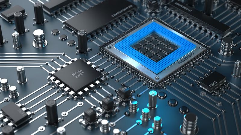
Electronic circuit chip (fabricated through chemical etching)
Introduction
In the intricate world of material fabrication and precision manufacturing, chemical etching is a powerful and versatile technique. This method, rooted in chemistry and metallurgy, has transcended its humble beginnings to become a cornerstone in creating intricate designs, fine patterns, and precision components. From the microscopic intricacies of electronic circuits to the artistic elegance of decorative metalwork, chemical etching plays a pivotal role in shaping the modern landscape of engineering and design.
Chemical etching, also known as photo etching, photochemical machining, or chemical milling, is a highly precise manufacturing process used in various industries. It is a precise manufacturing process that employs photochemical methods to selectively remove material from alloys, including stainless steel, to create intricate metal parts. It involves using acidic chemicals to remove material and create an etched pattern on a metal surface. This technique allows controlled dissolution of the alloy's surface by utilizing photoresist patterns, resulting in finely etched components. By leveraging photochemical etching, manufacturers achieve detailed designs and functional precision in producing metal parts, showcasing the versatility of this method in shaping alloy-based materials like stainless steel with unparalleled accuracy.
The process is known for its accuracy, repeatability, and ability to produce complex, intricate designs that would be difficult or impossible to achieve with other manufacturing methods. Chemical etching is used in various industries, including electronics, aerospace, automotive, medical, and more. Its applications range from the production of intricate electronic components to the creation of detailed aerospace parts. Understanding the principles and processes of chemical etching is crucial for anyone involved in these industries.[1]
History of Chemical Etching
The captivating history of chemical etching unfolds over centuries, dating back to the Middle Ages, where it played a crucial role in shaping burr-free armor and decorative items. This technique transitioned into an industrial context in the 19th century. The mid-19th century saw a transformative phase with the advent of photography, significantly influencing chemical etching. The introduction of photoresist, a light-sensitive material, became pivotal, allowing for precise control over the etching process on sheet metal, preventing burrs, and facilitating the creation of corrosion-resistant components.
As we progressed into the 20th century, the rise of electronics prompted advancements in chemical etching to meet the demand for complex and miniaturized metal parts. Automation and refinement became paramount, ensuring the production of intricate components with high precision and repeatability. Today, chemical etching is a critical process in manufacturing, from aerospace components to electronic circuits, emphasizing its importance in creating corrosion-resistant and lamination-free products.
A key milestone in the journey of chemical etching occurred in the mid-20th century with the development of microfabrication techniques, such as photolithography and etching. These techniques revolutionized the production of microelectronic devices and MEMS(micro-electromechanical systems), enabling the creation of intricate patterns on a microscopic scale in a burr-free manner.
Despite its extensive history, chemical etching continues to evolve. Ongoing advances in materials science, chemistry, and manufacturing technology further expand the capabilities of this technique, ensuring its vital role in crafting precise and burr-free metal parts while preventing corrosion and lamination. Looking ahead, the future of chemical etching appears dynamic, promising continued innovation in the manufacturing industry.[2]
The Science Behind Chemical Etching
Chemical etching is a complex process that relies on chemical reactions, material properties, and process control to achieve the desired results. At its core, chemical etching involves the selective removal of material from a substrate using a chemical solution, typically an acid. The process is controlled by applying a photoresist layer to the substrate, which protects the areas that should not be etched.
The choice of chemicals used in the etching process depends on the material and the desired etch rate. Common etchants include hydrochloric acid, nitric acid, and ferric chloride for metals like copper and potassium hydroxide for materials like silicon. The etching process can be further controlled by adjusting temperature, concentration, and agitation.[3]
Chemical Reactions Involved
The chemical reactions during the etching process are critical to its success. These reactions involve the interaction between the etchant and the material being etched, resulting in the dissolution of the material and the formation of byproducts.
For example, when etching copper with ferric chloride, the following reaction occurs:
Cu (s) + 2 FeCl3 (aq) → CuCl2 (aq) + 2 FeCl2 (aq)
In this reaction, solid copper (Cu) reacts with ferric chloride (FeCl3) to form copper(II) chloride (CuCl2) and ferrous chloride (FeCl2). The copper(II) chloride is soluble in the etching solution, removing the copper from the substrate.
Understanding the chemical reactions involved in the etching process is essential for optimizing the process and achieving the desired results. Factors such as etchant concentration, temperature, and agitation can all influence the rate and efficiency of these reactions and must be carefully controlled to ensure a successful etching process.
Role of Temperature and Pressure
Temperature and pressure play crucial roles in the chemical etching process, as they can significantly impact the rate and efficiency of the chemical reactions involved. Controlling these factors makes optimizing the etching process and achieving the desired results possible.
Temperature affects the etching process in several ways. First, it influences the solubility of the etchant and the byproducts formed during the etching process. Higher temperatures generally increase the solubility of these substances, allowing for faster dissolution of the material being etched. Second, temperature affects the rate of the chemical reactions involved in etching. Generally, increasing the temperature will increase the reaction rate, leading to faster etching. However, it is important to note that excessively high temperatures can cause undesirable side effects, such as increased etchant evaporation or damage to the photoresist layer.
Pressure also plays a role in etching, particularly in dry etching techniques. In dry etching, the pressure within the etching chamber can be adjusted to control the mean free path of the reactive species, which in turn affects the etching rate and selectivity. For example, lower pressures can result in a longer mean free path, allowing the reactive species to reach deeper into the substrate and achieve more anisotropic etching profiles. Conversely, higher pressures can lead to a shorter mean free path and more isotropic etching profiles.
In summary, temperature and pressure are critical factors in the chemical etching process, and their careful control is essential for achieving optimal results. By understanding the effects of these factors on the etching process, it is possible to fine-tune the process parameters and produce high-quality, precise components.
Types of Chemical Etching
Chemical etching can be broadly classified into wet etching and dry etching. Each type has advantages and disadvantages, and the choice between them depends on the application's specific requirements.
Wet etching is the traditional form of chemical etching, and it involves the use of liquid chemicals or etchants to remove material from the substrate. The substrate, covered with a patterned photoresist layer, is immersed in the etchant, and the areas of the substrate that are not protected by the photoresist are dissolved. Wet etching is a relatively simple and cost-effective process, and it can be used with a wide range of materials and etchants. However, it can be difficult to control the etching rate and profile with wet etching, which can generate large amounts of liquid waste.
On the other hand, dry etching uses gases or plasmas as the etching medium. The substrate is placed in a vacuum chamber, and the etching gas or plasma is introduced. The reactive species in the gas or plasma react with the substrate material, forming volatile byproducts that the vacuum system removes. Dry etching offers greater control over the etching rate and profile, and it can produce features with high aspect ratios and vertical sidewalls. However, dry etching processes are generally more complex and expensive than wet etching, requiring specialized equipment.
Wet Etching
Wet etching is a chemical etching process that uses liquid chemicals or etchants to remove material from a substrate. The process involves immersing the substrate in the etching solution, which is covered with a patterned photoresist layer. The areas of the substrate that are not protected by the photoresist are then dissolved by the etchant.
The choice of etchant depends on the substrate material and the desired etch rate. Common etchants include hydrochloric acid, nitric acid, ferric chloride for metals like copper and potassium hydroxide for materials like silicon. The etching rate can be controlled by adjusting the concentration of the etchant, the temperature, and the agitation.
One of the main advantages of wet etching is its simplicity. The process is relatively straightforward and does not require specialized equipment, making it a cost-effective option for many applications. However, wet etching also has its limitations. The process can be difficult to control, leading to etching rate and profile variations. Additionally, wet etching generates liquid waste, which must be properly managed to avoid environmental contamination.
Despite these challenges, wet etching remains a widely used technique in many areas of manufacturing and research, including semiconductor fabrication, microelectromechanical systems (MEMS) production, and materials science research.
Dry Etching
Dry etching is a type of chemical etching that uses gases or plasmas as the etching medium instead of liquid chemicals. The process occurs in a vacuum chamber, exposing the substrate to the etching gas or plasma. The reactive species in the gas or plasma react with the substrate material, forming volatile byproducts that the vacuum system removes.
The etching gas or plasma choice depends on the substrate material and the desired etch rate and profile. For example, fluorine-based gases are commonly used for etching silicon, while chlorine-based gases are used for etching metals. The etching rate and profile can be controlled by adjusting the gas flow rate, the power of the plasma, and the pressure in the vacuum chamber.
One of the main advantages of dry etching is the level of control it offers over the etching process. Because the etching occurs in a vacuum and the reactive species are highly directional, dry etching can produce features with high aspect ratios and vertical sidewalls. This makes it particularly suitable for applications that require precise patterning, such as the fabrication of microelectromechanical systems (MEMS) or advanced semiconductor devices.
However, dry etching also has its challenges. The process is more complex than wet etching and requires specialized equipment, such as a vacuum system and a plasma generator. This makes dry etching more expensive than wet etching. Additionally, the byproducts of dry etching can be hazardous and must be properly managed to ensure safety and environmental compliance.
Despite these challenges, dry etching is a critical technique in many areas of manufacturing and research. Its ability to produce precise and complex patterns makes it an indispensable tool in fabricating modern electronic devices, from microprocessors to memory chips.
Further reading: Dry Etching vs Wet Etching: A Comprehensive Comparison
Chemical Etching Process
The chemical etching process involves selective material removal from a substrate using a chemical solution. The process begins with preparing the substrate, followed by applying a photoresist layer, exposure, development of the photoresist, etching, and finally, removal of the photoresist.
The substrate, typically a metal or silicon wafer, is first cleaned to remove any surface contaminants that could interfere with the etching process. This is often done using a combination of chemical cleaning solutions and ultrasonic agitation. Once the substrate is clean, a photoresist layer is applied. The photoresist is a light-sensitive material that hardens when exposed to light. By selectively exposing the photoresist to light through a mask, it is possible to create a pattern on the substrate corresponding to the areas that should be etched.
After the photoresist has been exposed and developed, the substrate is immersed in the etching solution. The etching solution reacts with the exposed areas of the substrate, dissolving the material and creating the desired pattern. The rate and depth of etching can be controlled by adjusting factors such as the concentration of the etching solution, the temperature, and the agitation.
Finally, once the etching process is complete, the remaining photoresist is removed, leaving behind the etched substrate. The substrate is then rinsed and dried, ready for the next steps in the manufacturing process.[4] They are fully explained below:
Material Cleaning and Preparation:
Material cleaning and preparation are the foundational steps in the chemical etching process, crucial for achieving precise and reliable results. Before etching, meticulous cleaning of the metal surface is imperative to eliminate contaminants like oils or oxides that might impede the process. This meticulous cleansing ensures optimal adhesion of the subsequent photoresist layer and promotes uniform etching.
The preparation involves a series of steps, commencing with thoroughly cleaning the substrate using chemical solutions and ultrasonic agitation. The choice of cleaning solutions is tailored to the substrate type and the specific contaminants present. Following cleaning, the substrate undergoes a rinsing process, typically employing deionized water to eliminate any residual cleaning solution, ensuring a pristine surface for etching.
Once cleaned and dry, the substrate is poised for applying the photoresist. Applied through spin coating, the light-sensitive material is dispensed onto the substrate's center and then rapidly spun to achieve an even coating. Subsequent baking of the prepared substrate serves to harden the photoresist, preparing it for the upcoming stages of the etching process. This baking step removes lingering solvents from the photoresist, creating a clean and stable surface conducive to successful etching. These meticulous material cleaning and preparation steps set the stage for the intricate and precise chemical etching process.
Application of a Photoresist Layer:
The photoresist application is a pivotal phase in the intricate chemical etching process, where a light-sensitive photoresist material is meticulously applied to the metal surface. This critical step, essential for achieving precision in crafting intricate designs and patterns, embraces various versatile methods such as spraying, laminating, or dipping. The photoresist emerges as a protective layer on the metal components, delineating the areas to be etched and safeguarding the rest.
This protective layer plays a crucial role in the subsequent machine process, where precision and control are paramount. By selectively exposing the metal through photoresist, intricate prototypes, and finely detailed metal components are produced with unparalleled accuracy. The photoresist's adaptability and protective function make it instrumental in evolving sophisticated manufacturing, creating intricate designs and prototypes that meet the highest standards of precision and repeatability.
Exposure to Light:
The metal sheet, now adorned with photoresist, encounters a crucial phase as it basks in the exposure to ultraviolet (UV) light through a specialized photo tool or mask. This tool encapsulates the desired pattern or design, acting as the guiding maestro in this intricate process. Where the precise touch of ultraviolet light meets the photoresist, a sophisticated chemical reaction unfolds, inducing transformative alterations in the material's properties.
The incorporation of UV light enhances the precision of this phase, accentuating the control over the etching process. This orchestrated dance between ultraviolet light and the photoresist encapsulates the synthesis of artistry and chemistry, shaping the destiny of the metal sheet as it embarks on the journey toward a meticulously etched and intricately designed final product.
Development Process:
After exposure, the metal sheet embarks on a critical development process in the chemical etching journey. This essential stage involves the removal of unexposed or softened photoresist, revealing the underlying nickel alloy intricately shaped according to the desired pattern. This unveiling is pivotal for precision metal manufacturing, particularly in crafting precision parts.
The nuanced control over the development process ensures the selective dissolution or softening of the photoresist, leaving behind a meticulously etched canvas. This phase is paramount in applications requiring precision, such as creating precision parts or shims. The revealed nickel alloy surface, free from undesirable oxides, stands ready for the subsequent etching process, embodying the meticulous intricacies envisioned during the design.
Etching Process
The core of the chemical etching process lies in the etching step, a pivotal phase orchestrating the meticulous removal of material from the substrate, particularly crucial in creating precision prototypes. In this critical stage, the substrate, adorned with a meticulously developed photoresist pattern, submerges into a carefully chosen chemical etchant solution. The chemical alchemy unfolds as the etching solution reacts with exposed areas of the substrate, dissolving material and giving life to the desired pattern.
The choice of etching solution, tailored to the substrate material and the desired etch rate, is crucial in achieving optimal prototype outcomes. Ferric chloride finds its application in etching copper, while potassium hydroxide takes the lead for silicon. Precision is honed by adjusting the concentration, temperature, and agitation, thereby controlling the etching rate and achieving precise results within the specified etching time.
An indispensable aspect is adhesion, where the photoresist must securely bond to the metal surface for optimal results in the subsequent etching process. The proficiency of the chemical etchant is paramount, ensuring efficient material removal while preserving the integrity of the thin metal and types of metal involved. Moreover, this method starkly contrasts traditional hard tooling, offering advantages like enhanced flexibility and cost-effectiveness. Compared to laser cutting, metal etching excels in preserving the structural integrity of thin metals across various types.
Throughout this intricate journey, vigilance is paramount, ensuring the accurate transfer of the desired pattern onto the substrate for precise prototypes. Inspection techniques, including optical or scanning electron microscopy, are crucial in overseeing this process. With the completion of the etching process, the substrate emerges from the solution, undergoes rinsing, and stands ready for the subsequent stages in the manufacturing process, embodying the precision, versatility, and artistry inherent in chemical etching for prototypes.
Post-Etching Processes
After the etching process, the substrate undergoes several post-etching processes to finalize the etched pattern and prepare the substrate for subsequent manufacturing steps. These processes include stripping, cleaning, and inspection.
Stripping:
Stripping involves the meticulous removal of the remaining photoresist using a chemical stripper. This dissolves the photoresist without affecting the substrate or the etched pattern. The choice of the stripper, be it acetone, N-methyl-2-pyrrolidone (NMP), or oxygen plasma, depends on the photoresist type and substrate material. For example, acetone or N-methyl-2-pyrrolidone (NMP) can strip positive photoresists, while oxygen plasma is often used to strip negative photoresists.
Cleaning:
After stripping, the substrate undergoes rigorous cleaning to eliminate residual stripper or etching solution. A series of rinses with deionized water and other cleaning solutions ensure thorough cleaning. This step is critical for preventing substrate contamination, particularly for applications with stringent lead times.
Inspection:
The final step in the post-etching process is inspection. The etched substrate is inspected to verify the accuracy and quality of the etched pattern. This can be done using various inspection techniques, such as optical or scanning electron microscopy. The inspection process allows for detecting any defects or errors in the etching process, such as under-etching or overreaching, and provides feedback for process control and optimization.
The post-etching processes are critical for ensuring the quality and accuracy of the etched components. By carefully controlling these processes, producing high-quality, precise components that meet the stringent requirements of modern electronics and other high-tech industries is possible. Integrating water jet, wire EDM, and metal etching processes into post-etching stages ensures that manufacturers achieve high-quality, precise components with varying metal thicknesses, all while meeting stringent lead times in diverse industrial applications.
Further reading: Plasma Etching: A Comprehensive Guide to the Process and Applications
Applications of Chemical Etching
Chemical etching finds extensive application across various industries due to its ability to create precise and complex patterns on a substrate. The process is particularly valuable in industries requiring high precision and accuracy, such as electronics, aerospace, and medical devices.
In the electronics industry, chemical etching is used in the fabrication of printed circuit boards (PCBs), integrated circuits (ICs), and microelectromechanical systems (MEMS). The process allows for the creation of intricate patterns and structures on a microscopic scale, which is essential for the functioning of these devices.
The aerospace industry uses chemical etching to produce complex geometries and high-precision components. These components must withstand extreme conditions, such as high temperatures and pressures, making the precision and accuracy provided by chemical etching crucial.
In the medical device industry, chemical etching is used to manufacture devices such as stents, catheters, and surgical instruments. The process allows for the creation of features with high precision and accuracy, which is critical for the performance and safety of these devices.[5]
Electronics Industry
In the electronics industry, chemical etching plays a crucial role in the fabrication of various devices, including printed circuit boards (PCBs), integrated circuits (ICs), and microelectromechanical systems (MEMS).
PCBs are used in virtually all electronic devices, from computers and smartphones to home appliances and industrial equipment. Chemical etching creates the conductive pathways, or traces, on the PCB that connect the various electronic components. The process allows for the creation of intricate patterns with high precision, which is essential for the functioning of the PCB.
Integrated circuits, or microchips, are the heart of modern electronics. They contain millions or billions of transistors and other electronic components integrated into a single silicon chip. Chemical etching is used in several steps of the IC fabrication process, including patterning the silicon substrate and creating the metal interconnects that link the various components.
Microelectromechanical systems, or MEMS, are miniature devices that combine mechanical and electrical components. They are used in various applications, from car airbag sensors to projection systems in digital projectors. Chemical etching creates tiny mechanical structures in MEMS devices, such as cantilevers, diaphragms, and gears.
The precision and accuracy provided by chemical etching and its ability to create complex patterns on a microscopic scale make it an indispensable tool in the electronics industry.
Aerospace Industry
The aerospace industry is another sector where chemical etching is extensively utilized. The production of components for aircraft, spacecraft, and satellites often requires the creation of intricate patterns and structures with high precision, which is where chemical etching comes into play.
One of the key applications of chemical etching in the aerospace industry is producing heat exchangers. These are critical components used in aircraft and spacecraft for thermal management. They consist of a complex network of channels through which coolant flows to dissipate heat. Chemical etching creates these channels with high precision, ensuring optimal heat exchanger performance.
Chemical etching is also used to fabricate shims, which are thin materials that fill gaps or adjust fits in aerospace assemblies. Shims often have complex shapes and must fit precisely in the assembly, which makes chemical etching an ideal method for their production.
Another application is in the production of fuel cell components for spacecraft. Fuel cells generate electricity through a chemical reaction, requiring components with intricate patterns and high surface area to function efficiently. Chemical etching is used to create these patterns, enhancing the performance of the fuel cell.
In the aerospace industry, the precision and accuracy provided by chemical etching are critical. The components produced are often used in extreme conditions, such as high temperatures and pressures, and any deviation from the specified dimensions can lead to failure of the component or even the entire system. Therefore, the ability of chemical etching to produce components with high precision and accuracy makes it an invaluable tool in the aerospace industry.

Advantages of Chemical Etching
Chemical etching offers several advantages, making it a preferred method for creating intricate patterns and structures on a substrate. One of the primary advantages is its precision. Chemical etching can produce features with high accuracy, often within a tolerance of a few micrometers. This level of precision is crucial in industries such as electronics and aerospace, where components often have complex geometries and must fit precisely in assemblies.
Another advantage of chemical etching is its versatility. The process can be used with various materials, including metals, semiconductors, and ceramics. This makes it a flexible tool that can be adapted to different applications and industries. Furthermore, the choice of etchant can be tailored to the specific material and the desired etch rate and profile, providing further control over the etching process.
Chemical etching is also a non-contact process, meaning it does not physically touch the substrate during the etching process. This eliminates the risk of mechanical damage to the substrate, which can be a concern with other fabrication methods. The non-contact nature of chemical etching also means that it does not generate mechanical stress in the substrate, which can lead to deformation or failure of the component.
The ability of chemical etching to create complex patterns and structures on a microscopic scale is another significant advantage. This capability is essential in fabricating modern electronic devices, such as integrated circuits and microelectromechanical systems containing millions or billions of features on a single chip.
Finally, chemical etching is a cost-effective process, especially for high-volume production. The process can be easily automated, allowing for high throughput and low per-unit costs. The cost-effectiveness of chemical etching, combined with its precision, versatility, and ability to create complex features, makes it a valuable tool in many areas of manufacturing and research.
Limitations and Challenges of Chemical Etching
While chemical etching offers numerous advantages, it has limitations and challenges. Understanding these limitations is essential for selecting the appropriate manufacturing process for a given application and optimizing the etching process to achieve the desired results.
One of the primary limitations of chemical etching is its material compatibility. The process is most effective with metals and certain types of plastics, but it may not be suitable for materials resistant to the etching chemicals or damaged by the chemicals. For example, some ceramics and composites may not be compatible with chemical etching, requiring alternative fabrication methods.
Another challenge associated with chemical etching is controlling the etching rate and profile. While the process offers high precision, achieving the desired etch rate and profile can be difficult, particularly for complex geometries or materials with varying etch rates. Factors such as etchant concentration, temperature, and agitation must be carefully controlled to ensure consistent etching across the substrate.
The generation of waste is another concern with chemical etching. The process produces liquid waste from spent etchants and rinse water, which must be properly managed to avoid environmental contamination. This can add to the overall cost and complexity of the process, particularly for large-scale production.
Additionally, chemical etching can be sensitive to substrate material variations, such as grain structure changes or impurities. These variations can lead to inconsistencies in the etching process, resulting in defects or non-uniform etching. Careful material selection and process control are necessary to minimize these issues.
Finally, while chemical etching is a low-cost process for high-volume production, it may not be the most economical choice for low-volume or one-off production. The cost of creating the necessary masks and setting up the etching process can be prohibitive for small-scale production, making alternative fabrication methods more attractive in these cases.[6]
Conclusion
Chemical etching is a versatile and valuable manufacturing process that enables the creation of intricate patterns and structures on various substrates. Its precision, accuracy, and adaptability make it an essential tool in industries such as electronics, aerospace, and medical devices. Chemical etching is critical in producing high-quality, precise components integral to modern technology despite its limitations and challenges. As materials science and manufacturing technology continues to advance, chemical etching capabilities and applications will likely expand, further solidifying its importance in the manufacturing landscape.
Frequently Asked Questions (FAQs)
Q: What is chemical etching? A: Chemical etching is a process that uses acidic chemicals to selectively remove material from a substrate, creating intricate patterns and structures.
Q: What are the main types of chemical etching? A: The two main types of chemical etching are wet etching, which uses liquid chemicals, and dry etching, which uses gases or plasmas.
Q: What industries use chemical etching? A: Chemical etching is widely used in electronics, aerospace, and medical devices, where high precision and accuracy are required.
Q: What are the advantages of chemical etching? A: Advantages of chemical etching include its precision, versatility, non-contact nature, ability to create complex patterns, and cost-effectiveness for high-volume production.
Q: What are the limitations and challenges of chemical etching? A: Limitations and challenges of chemical etching include material compatibility, control of etching rate and profile, waste generation, sensitivity to substrate variations, and cost considerations for low-volume production.
Reference
Qualitech, 2016. Introduction to Chemical Etching. Available at: https://www.qualitetch.com/introduction-chemical-etching/https://www.qualitetch.com/introduction-chemical-etching/ (Accessed: January 14, 2024).
Etch Tech, n/a. A History of Etching and its place in Modern Manufacturing. Available at: https://www.etch-tech.co.uk/about/more-about-etching/ (Accessed: January 14, 2024).
Heimann, R.B. (1982). Principles of Chemical Etching — The Art and Science of Etching Crystals. In: Grabmaier, J. (eds) Silicon Chemical Etching. Crystals, vol 8. Springer, Berlin, Heidelberg. https://doi.org/10.1007/978-3-642-68765-5_3
Interplex, 2019. Chemical Etching: Understanding the Process and its Applications. Available at: https://interplex.com/chemical-etching-guide/ (Accessed: January 14, 2024).
United Western Enterprises, Inc, 2023. Chemical Etching: What Is It and How Does It Work? Available at: https://www.uweinc.com/chemical-etching-what-is-it-and-how-does-it-work/#:~:text=Applications%20of%20Chemical%20Etching&text=Common%20electronic%20components%20fabricated%20via,components%20used%20in%20aerospace%20applications
J. W. Judy, Microfabrication: A Practical Guide, 2nd ed. Boca Raton, FL: CRC Press, 2016.
in this article
1. Introduction2. History of Chemical Etching3. The Science Behind Chemical Etching4. Types of Chemical Etching5. Chemical Etching Process6. Post-Etching Processes7. Applications of Chemical Etching8. Advantages of Chemical Etching9. Limitations and Challenges of Chemical Etching10. Conclusion11. Frequently Asked Questions (FAQs)12. Reference