A Comprehensive Guide to FPGA Development Boards
Choosing, using, and advancing with your first FPGA development board. This guide demystifies FPGA development boards for students, hobbyists, and engineers. Learn how to select the right starter kit, set up the toolchain, complete your first project, and troubleshoot hardware and software issues.

26 May, 2026. 19 minutes read
Key Takeaways
Understand development boards – An FPGA development board integrates an FPGA device with power regulation, configuration flash, oscillator, programming/debug interface, and I/O connectors. These components let you experiment without the burden of designing a base board from scratch.
Selection criteria matter – Device capacity (logic cells, DSP blocks, block RAM), supported toolchain, onboard peripherals, and price tier all influence the choice of your first FPGA starter kit.
Free and open tools exist – Vendor suites such as Vivado (AMD), Quartus Prime (Intel), Radiant (Lattice), and Libero (Microchip) offer free tiers, while open-source flows using Yosys and nextpnr provide vendor‑agnostic alternatives.
Hands-on projects accelerate learning – Start with a blinking LED design, then progress to serial interfaces, video outputs, or soft-core CPUs to understand clocking, I/O constraints, and HDL design practices.
Debugging is integral – Simulators, embedded logic analyzers (Vivado ILA or Intel SignalTap), and proper verification methodology help identify timing and functional issues before and after synthesis.
Plan your progression – After mastering entry‑level boards, explore SoC boards, soft-core processors, DSP, and high‑level synthesis, and consider formal training or certification.
Introduction
Imagine transforming an idea for a custom CPU, a video processor, or a real-time filter into functioning hardware that you can hold in your hands. Field‑programmable gate arrays (FPGAs) make this possible by allowing you to configure programmable logic blocks and interconnects to implement custom digital circuits gates to implement digital circuits. Unlike bare FPGA chips or standard microcontrollers, a development board packages the FPGA with power supplies, clocks, configuration memory, I/O connectors, and programming hardware. This ready‑to‑use platform removes the steep hardware hurdles and allows you to focus on learning hardware description languages (HDLs) such as Verilog or VHDL, exploring design flows, and experimenting with embedded systems.
This article is not a generic product overview; it's a practical journey from choosing your first FPGA development board to building your first design and beyond. We'll compare popular entry-level and intermediate boards, discuss proprietary and open toolchains, walk through a blinking‑LED project, share debugging tips, and highlight paths to professional FPGA work.
What is an FPGA Development Board?
An FPGA device is essentially an integrated circuit sea of configurable logic blocks (CLBs — or equivalent structures across vendors) connected through a programmable interconnect. On its own, the chip needs regulated power rails, configuration memory to load the bitstream at power‑up, oscillators to provide clock signals, and a programming interface such as JTAG. An FPGA development board combines these essentials with peripherals and connectors:
FPGA device – The heart of the board. Popular families include AMD Artix‑7 and Spartan, Intel (formerly Altera) Cyclone V, Lattice iCE40/ECP5, Efinix Trion, and Microchip PolarFire. The amount of logic (LUTs/logic elements), embedded memory blocks (BRAM or block RAM), multipliers/DSP slices, and built‑in hard cores (e.g., ARM processors or high‑speed transceivers) define the board's computational capacity.
Configuration flash and programming interface – Boards include a serial flash that stores the bitstream and a USB‑based programmer (e.g., Digilent USB‑JTAG, FTDI FT2232H, or BL702) for downloading configurations, eliminating the need for external programmers.
Clocks and power – Oscillators generate system clocks (commonly 12 MHz, 50 MHz, or 100 MHz) and regulators supply stable core and I/O voltages. Most FPGAs also include on-chip PLLs or DCMs to derive multiple clock frequencies from a single source.
Peripherals and I/O connectors – LEDs, switches, seven‑segment displays, USB‑UART bridges, Ethernet PHYs, analog‑to‑digital converters (for example, Xilinx XADCor an external ADC), VGA/HDMI ports, and audio codecs allow you to build interactive projects. Expansion connectors (Pmod™, Arduino, FMC, or Raspberry Pi headers) provide access to additional sensors or high‑speed interfaces.
Software toolchain support – Each FPGA vendor provides a design suite — such as Vivado (AMD/Xilinx), Quartus Prime (Intel), or Radiant (Lattice) — to synthesize, place, route, and program the device. Open-source flows using Yosys and nextpnr offer vendor-agnostic alternatives. Active community forums and example projects can significantly shorten the learning curve for beginners.
Using a development board removes the complexity of designing a custom PCB or managing messy wiring on a breadboard . It lets you dive straight into writing HDL, understanding timing constraints, and building real hardware designs, making it ideal for learning and prototyping.
Recommended Reading: FPGA Programming: Theory, Workflow, and Practical Implementations
Anatomy of a Development Board
To choose and use a board effectively, you need to understand its major components. The general layout of many boards resembles this pattern:
FPGA die – The specific chip, such as an AMD Artix‑7 XC7A35T (Basys 3) or Intel Cyclone V SoC (DE10‑Nano), contains tens of thousands of look‑up tables and flip‑flops. Higher‑end chips add DSP slices for multiplications and high‑speed transceivers for gigabit I/O. The chip is typically housed in a BGA package (smaller devices may use QFN) and soldered at the center of the PCB.
Configuration flash – A Quad‑SPI or SPI serial flash stores the configuration bitstream. On power‑up, the chip loads this file automatically. Boards may support partial reconfiguration or multiple stored bitstream images for different configurations.
Oscillators and PLLs – Crystal oscillators provide reference frequencies. Internal PLLs multiply or divide these reference frequencies to generate the system clocks required by the design. For example, the Tang Nano 9K board uses a 27 MHz oscillator and two PLLs [4].
Programming/debug header – A dedicated USB connector with FTDI FT2232H, Digilent USB‑JTAG, or Microchip FlashPro provides JTAG programming and often a USB‑UART bridge for serial communication. Some boards supply on‑board logic analyzer interfaces such as Digilent's integrated JTAG-SMT module.
Power management – Buck converters and linear regulators generate core voltages (1.0–1.2 V) and I/O voltages (1.8 V, 3.3 V). Jumpers or switches may select supply sources (USB vs. external). Pay attention to current ratings if you plan to power external hardware.
User I/O – Arrays of LEDs, switches and buttons help verify simple designs without external hardware. Seven‑segment displays and rotary encoders are common on educational boards.
Expansion headers – Pmod connectors (12-pin, two rows of 6) expose eight digital I/O signals alongside power and ground pins.; Arduino/chipKIT headers support shield ecosystems; FMC (FPGA Mezzanine Card) connectors offer high‑speed I/O; Raspberry Pi‑style headers add compatibility with camera modules and HATs.
Peripheral interfaces – Many boards include USB 2.0/3.0, Gigabit Ethernet, HDMI/VGA and I²C/SPI connectors. SoC boards add hard-ARM processor cores and DDR memory chips for running Linux and general-purpose processors.
Understanding this anatomy helps you evaluate whether a board meets your project's requirements and provides the necessary interfaces.
How to Choose Your First FPGA Development Board
Your first FPGA board should balance affordability, learning value and project requirements. Consider the following criteria:
Device resources
Logic capacity – Measured in logic cells, LUTs, or logic elements. A modest board like the Lattice iCEstick with an iCE40HX1K FPGA offers 1,280 logic cells [3]. This is sufficient for simple combinational circuits or counters. A mid‑range board, such as the Digilent Basys 3, features an Artix‑7 XC7A35T with 33,280 logic cells (5,200 slices) [1], which supports soft‑core CPUs or small digital signal processing (DSP) filters. High‑end boards like the AMD Kria KV260 Vision AI Starter Kit provide 256 K system logic cells and 1.2 K DSP slices [8] for image‑processing acceleration.
Block RAM and DSP – Look for on‑chip memory capacity (BRAM or block RAM). Basys 3 contains 1.8 Mbits of block RAM [1], whereas the DE10‑Nano's Cyclone V SoC
packs 4450 Kb of memory [5]. DSP slices (18×18 multipliers) are essential for filters and neural network layers; the Arty A7‑100 has 240 DSP slices [2].
Hard processors and transceivers – SoC FPGAs embed ARM or RISC‑V cores. The DE10‑Nano features dual‑core Cortex‑A9 processors and integrated peripherals; the PolarFire SoC Discovery Kit uses an MPFS095T device with five 64‑bit RISC‑V cores and 93 K logic elements [7]. High‑speed transceivers enable PCIe or HDMI; the PolarFirekit also provides four 12.7 Gbps SerDes lanes [7].
Toolchain and Software Support
Vendor toolchains vary in features, licensing and ease of use:
AMD Vivado Design Suite – Used for Artix‑7, Kintex‑7 and Zynq devices. The WebPACK/Standard edition is free and does not require a license for most entry‑level devices like the Artix‑7 and Zynq‑7000 boards. Basys 3 and Arty A7 manuals confirm that designs can be created with the free Vivado WebPACK license [1][2]. Vivado integrates synthesis, implementation, hardware debugging and IP generation.
Intel Quartus Prime – The Lite Edition requires no license and supports Cyclone V/10 devices [10]. The Standard/Pro editions are paid but include advanced timing analysis and IP generation. Quartus includes Platform Designer and the Nios II/Nios V soft‑core processor tools.
Lattice Radiant and Diamond – Lattice Radiant supports newer Nexus and Avant families. A free license allows design and evaluation for all Radiant‑supported devices [11]. A subscription license adds optimization and multi‑core compilation [11]. The older Diamond suite supports iCE40 and ECP5 devices; it is typically available free with registration.
Microchip Libero SoC – Required for PolarFire and SmartFusion families. Microchip offers a free Silver license for PolarFire devices up to a certain logic capacity [9]. Paid Gold and Platinum licenses enable larger devices and additional IP.
Open-source flows – Projects such as Yosys and nextpnr integrate synthesis and place-and-route respectively. They support families like Lattice iCE40 (Project IceStorm), Lattice ECP5 (Project Trellis) and some AMD Artix devices [12]. These flows are ideal for educational projects, because they avoid vendor lock‑in and run on Linux without registration. However, they may lack timing analysis accuracy or device support for high‑end chips.
Further reading: The Ultimate Guide to ASIC Design: From Concept to Production
On-board Peripherals and Expansion
Look for features aligned with your interests:
Educational boards like Basys 3 include 16 switches, 16 LEDs, five pushbuttons, a four‑digit seven‑segment display and VGA output [1]. They are perfect for digital logic labs.
Maker‑oriented boards such as the Arty A7 offer Pmod and Arduino connectors, Ethernet, USB‑UART, RGB LEDs and DDR3 memory [2]. They support MicroBlaze soft‑core CPU projects.
Low‑power boards like the iCEstick use a thumb‑drive form factor and provide five user LEDs, an IrDA transceiver and a Pmod connector [3]. They're ideal for portable or wearable projects.
SoC boards like DE10‑Nano or Kria KV260 come with DDR memory, Ethernet, HDMI, SD card and expansion headers. They run Linux or RTOS on embedded processors and integrate heavy DSP.
Community and Documentation
Good documentation and active communities are invaluable. Boards like the ZedBoard have thriving forums and open‑source examples. Manuals for Basys 3, Arty A7 and DE10‑Nano are available and comprehensive. Check for example projects, university support and accessible tutorials.
Budget Tiers
Tier | Example board | Approximate cost | Highlights |
Entry (≤ €100) | Lattice iCEstick | ~€50 | Tiny iCE40HX‑1K FPGA (1280 logic cells), USB form factor, five LEDs, Pmod connector [3]; runs open‑source IceStorm toolchain. |
Sipeed Tang Nano 9K | ~€20–30 | GW1NR‑LV9Q FPGA with 8,640 LUT4 and 468 Kbit block SRAM, HDMI, micro‑SD slot, six LEDs [4]; GOWIN EDA and open‑source support. | |
Mid (≈ €150–€250) | Digilent Basys 3 | ~€160 | Artix‑7 XC7A35T with 33 K logic cells and 90 DSP slices, 16 switches, 7‑segment display, VGA, Pmod connectors [1]. |
Digilent Arty A7‑35/100 | €150–€220 | Artix‑7 with up to 15,850 slices and 240 DSP slices; 256 MB DDR3L, Ethernet, USB‑UART, four RGB LEDs and Arduino shield header [2]. | |
Upper-mid (≈ €300–€500) | Terasic DE10‑Nano | ~€190 | Cyclone V SoC with 110 K logic elements, 5.6 Mb memory, 224 multipliers, dual‑core ARM Cortex‑A9, 1 GB DDR3, Ethernet and HDMI [5]. |
Advanced (≥ €500) | ZedBoard | ~€400 | Zynq‑7020 SoC with 85 K logic cells and dual Cortex‑A9; 512 MB DDR3, 256 Mb QSPI flash, HDMI, VGA and audio outputs [6]. |
AMD Kria KV260 | ~€250–€350 | Vision AI board with 256 K logic cells, 144 block RAM, 64 UltraRAM blocks, 1.2 K DSP slices and 4 GB DDR memory [8]; multiple MIPI camera ports and DisplayPort™ output. | |
Microchip PolarFire SoC Discovery Kit | ~€120 | MPFS095T SoC with 93 K logic elements, 292 MAC blocks and 308 memory blocks, Raspberry Pi and mikroBUS connectors [7]. |
Note: Prices are approximate and vary by region and distributor. Check official vendor sites for current pricing.
Choose a board that fits your budget and leaves headroom for learning. For first‑time learners, an entry or mid‑tier board suffices. Advanced boards come with SoCs and specialized I/O for specific applications like automotive ADAS systems, vision, or motor control.
Recommended reading: Verilog vs VHDL: A Comprehensive Comparison
Top FPGA Development Boards for Beginners
Let's examine some popular boards in more detail.
Lattice iCEstick
FPGA: Lattice iCE40HX‑1K (1,280 logic cells, 64 Kbit RAM, 95 I/Os) [3].
Features: Thumb‑drive form factor with five user LEDs, Pmod connector, IrDA transceiver, 12 MHz oscillator, and 32 Mbit SPI flash [3]. The FTDI 2232H provides programming and USB‑UART.
Toolchain: Works with iCEcube2 and Diamond Programmer; fully supported by the open‑source IceStorm/Yosys/nextpnr flow.
Use case: Ideal for learning FPGA basics, simple digital logic, open‑source tool experimentation, or portable projects.
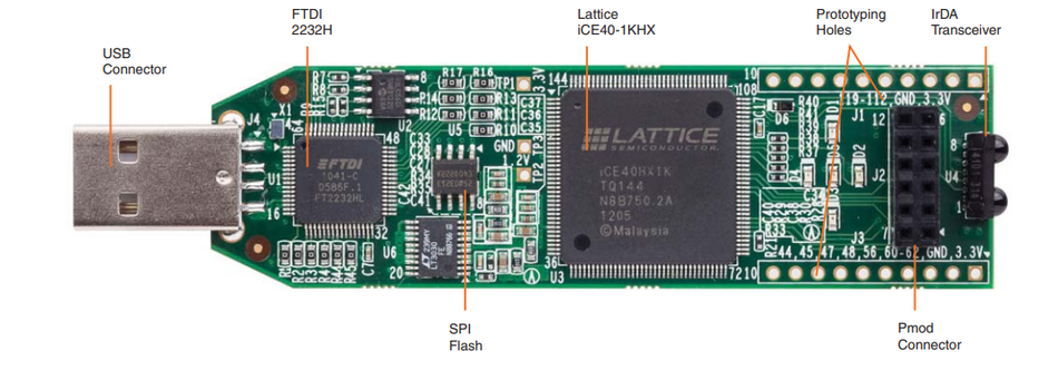
Sipeed Tang Nano 9K
FPGA: GOWIN GW1NR‑LV9Q with 8,640 LUT4s, 6,480 registers, 468 Kbit block SRAM, 20 multipliers, and 2 PLLs [4].
Features: 27 MHz oscillator, mini‑HDMI port for video output, micro‑SD slot, USB‑C for power and programming via onboard BL702 chip, and six user LEDs [4].
Toolchain: Supports Gowin EDA; open‑source support via project Apicula and nextpnr‑gowin is emerging.
Use case: Great for experimenting with video signals (VGA/HDMI) and running RISC‑V soft cores (e.g., PicoRV) [4]. Its low price makes it a fun entry-level board.
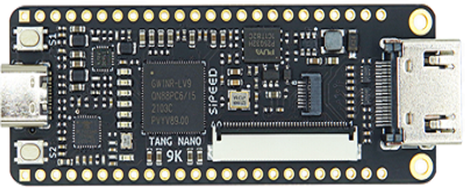
The Tang Nano 9K. Source: Sipeed
Digilent Basys 3
FPGA: AMD Artix‑7 XC7A35T with 33,280 logic cells, 1.8 Mbit block RAM and 90 DSP slices [1].
Features: 16 switches, 16 LEDs, five pushbuttons, four-digit seven‑segment display, three Pmod connectors, XADC header, 12‑bit VGA output and a USB‑UART bridge [1]. The board is powered via USB and includes an on‑board Digilent USB‑JTAG programmer.
Toolchain: Supports Vivado Design Suite; the free WebPACK edition fully supports this device [1].
Use case: Perfect for digital design labs and universities. The on‑board peripherals allow you to create counters, games, state machines, and simple video projects.
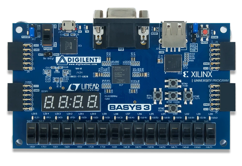
Digilent Basys 3. Source: Digilent
Digilent Arty A7 (35T and 100T variants)
FPGA: Artix‑7 35T or 100T with 5,200 slices (15,850 slices for the 100T) and up to 4,860 Kbit block RAM [2].
Features: 256 MB DDR3L memory, 16 MB Quad‑SPI flash, Gigabit Ethernet, USB‑UART, four switches/buttons, four LEDs plus four RGB LEDs, Pmod headers, and Arduino/chipKIT shield connector [2].
Toolchain: Vivado WebPACK; MicroBlaze soft‑core CPU supported via the free license [2].
Use case: Versatile board for running soft‑core CPUs (MicroBlaze), Ethernet‑connected IoT projects, or small SoC designs.
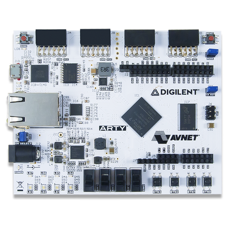
Digilent Arty A7 Board. Source: Digilent
Terasic DE10‑Nano
FPGA: Intel Cyclone V SE SoC with 110K logic elements, 5570 Kbits embedded memory, 224 18×19 multipliers and 112 DSP blocks [5].
Features: Dual‑core ARM Cortex‑A9 processor, 1 GB DDR3 memory, microSD card, Arduino header, Gigabit Ethernet, USB OTG, and two 40‑pin GPIO headers [5].
Toolchain: Supports Intel Quartus Prime Lite (free) and standard/higher tiers. The board also comes with the OpenCL SDK and can run Linux.
Use case: Suitable for hybrid FPGA/CPU projects, high‑performance DSP, and hardware acceleration. Popular for emulators (MiSTer project) and embedded Linux development.
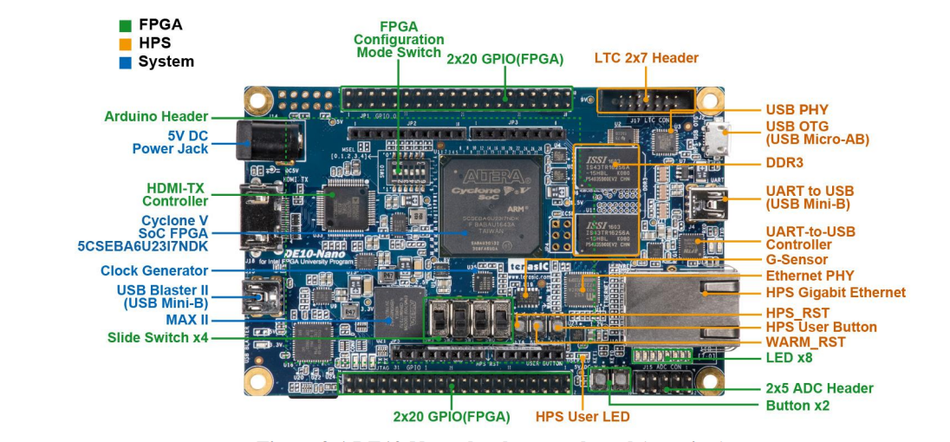
ZedBoard
FPGA: AMD Zynq‑7020 SoC with 85K logic cells, 53,200 LUTs, and dual 667 MHz Cortex‑A9 cores [6].
Features: 512 MB DDR3 memory, 256 Mb Quad‑SPI flash, Gigabit Ethernet, USB OTG and USB‑UART, HDMI and VGA outputs, audio codec, 128×32 OLED display, and multiple expansion headers [6].
Toolchain: Vivado Design Suite; community uses PetaLinux for embedded Linux. Free WebPACK supports Zynq‑7000 devices.
Use case: Great for embedded Linux, combined FPGA/ARM projects, and moderate DSP applications. The strong community and numerous example designs make it appealing.
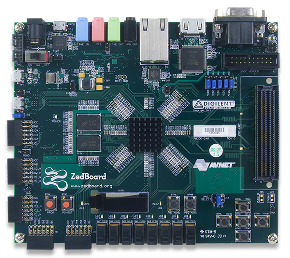
ZedBoard is a low-cost development board for the AMD Zynq™ 7000 all programmable SoC. Source: Digilent
Microchip PolarFire SoC Discovery Kit
FPGA: MPFS095T SoC with 93K logic elements, 292 18×18 MAC blocks and 308 20 Kbit RAM blocks [7].
Features: Quad‑core RISC‑V application cores plus a monitor core, Raspberry Pi 40‑pin header, mikroBUS connector, DDR4 memory, USB‑C power and multiple clocks. The kit comes pre‑programmed with a DSP demo that uses the FPGA's MAC blocks for FIR/FFT processing [7].
Toolchain: Microchip Libero SoC design suite; the free Silver license supports devices up to a certain capacity [9]. SoftConsole enables software development for the RISC‑V cores.
Use case: Ideal for exploring RISC‑V SoC FPGAs, experimenting with real‑time DSP and evaluating Microchip's low power, non‑volatile FPGA technology.
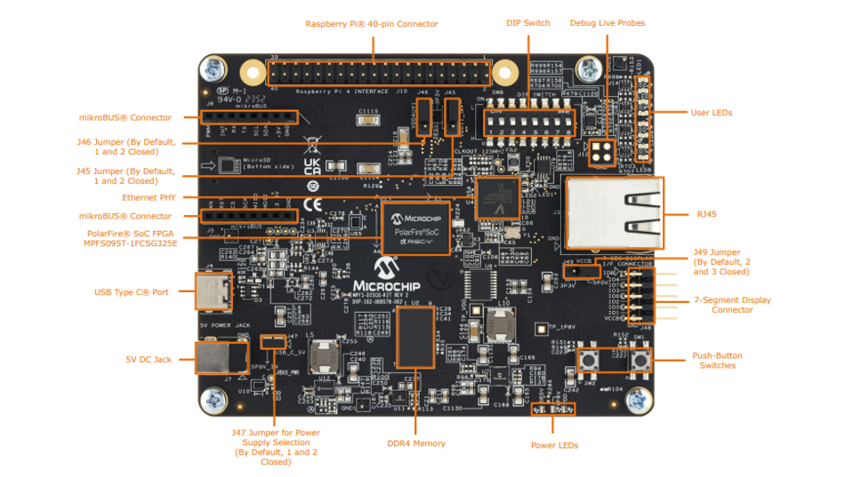
AMD Kria KV260 Vision AI Starter Kit
FPGA: Zynq UltraScale+ MPSoC K26 (industrial variant) with 256 K logic cells, 144 block RAM blocks, 64 UltraRAM blocks and 1.2 K DSP slices [8].
Features: 4 GB DDR4 memory, 512 Mb QSPI boot flash, SDHC card, Gigabit Ethernet, four USB 3.0 ports, MIPI camera interfaces (two OnSemi IAS and one Raspberry Pi), AP1302 image sensor processor, DisplayPort 1.2a, HDMI 1.4, Pmod interface and hardware root of trust [8].
Toolchain: Vivado/Vitis; the board ships with a pre‑built smart‑camera application. The system is optimized for AI inference and leverages AMD's Vitis AI framework.
Use case: Suitable for machine vision, edge AI and robotics. The board demonstrates how FPGAs accelerate deep‑learning models while running Linux on the embedded quad‑core ARM.
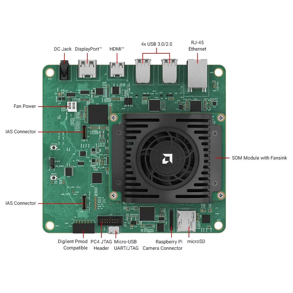
Kria KV260 Vision AI Starter Kit. Source: AMD
Setting Up the Toolchain
Installing Vendor Tools
Follow the vendor's installation procedure and consider licensing:
Vivado (AMD) – Download the unified installer from AMD's website and choose the Standard edition (formerly WebPACK). Create an AMD account, but no license is required for Artix‑7 and Zynq‑7000 devices. Use Vivado's project wizard to target your board.
Quartus Prime (Intel) – Download the Lite edition, which is license‑free [10]. Select Cyclone V device support. Installation includes the USB‑Blaster II driver for programming.
Radiant and Diamond (Lattice) – Use the free license of Radiant to design and evaluate devices [11]. The license file is node‑locked; request it via Lattice's website. For iCE40/ECP5 boards, download Lattice Diamond or rely on the open‑source IceStorm toolchain.
Libero SoC (Microchip) – Register on Microchip Direct and request a free Silver license for PolarFire devices up to a certain size[9]. Download the installer and follow the licensing guide. Libero integrates Synopsys Synplify and ModelSim ME, so it requires more disk space.
Efinix Efinity – For Trion boards, download the Efinity IDE and request a free evaluation license from Efinix. Efinity includes synthesis, place and route and bitstream generation.
GOWIN EDA – For Tang Nano boards, download Gowin IDE; a free license is available after registration.
Exploring Open‑source Toolchains
Open‑source flows have matured and support many entry‑level devices:
Yosys performs logic synthesis to an intermediate representation. Combined with nextpnr for place and route, you can target Lattice iCE40, ECP5, and certain AMD devices via Project IceStorm (iCE40), Project Trellis (ECP5), and Project X-Ray (Artix‑7). [12].
Verilator offers fast cycle‑accurate simulation using C++, and Icarus Verilog provides simpler simulation. Pair them with GTKWave to view waveforms.
LiteX and Migen frameworks let you build SoC architectures in Python; they can target Lattice, AMD, and Efinix boards. For example, you can generate a RISC‑V soft core (VexRiscv) and a peripheral set for the Tang Nano or ECP5 boards.
While open‑source toolchains provide transparency and avoid license restrictions, they often lack vendor IP and advanced timing closure features. Use them for experimentation and learning, but consider vendor tools when approaching timing-critical designs.
Your First Project: Blinking an LED
Nothing beats the thrill of seeing hardware respond to your code. A classic first project is toggling an LED at a visible rate. Here's a general procedure using the Basys 3 board and Vivado; adapt it to your board and toolchain.
Project Setup
Create a new project – In Vivado, select "Create Project," name it blinky, and specify the project location. Choose "RTL Project" and enable Verilog.
Select the FPGA part or board – In the boards tab, pick Basys 3 (xc7a35tcpg236‑1). If your board isn't listed, choose the device package manually.
Add source files – Create a new Verilog file named blinky.v.
Define the top‑level module – Write a module with inputs for the clock (clk) and outputs for the LED. Many boards expose a 100 MHz or 12 MHz oscillator on a dedicated pin. A simple clock divider reduces the high frequency to a human‑visible blink rate.
module blinky(
    input wire clk,       // system clock
    output reg led        // onboard LED
);


    // Parameter to adjust the blink period
    parameter DIVIDER = 26'd50_000_000; // ~0.5s at 100 MHz


    reg [25:0] counter = 0;


    always @(posedge clk) begin
        if (counter == DIVIDER) begin
            counter <= 0;
            led <= ~led;
        end else begin
            counter <= counter + 1;
        end
    end
endmodule
Create a constraints file – Assign the FPGA pins to the board's LED and clock. In Vivado, import the Basys 3 master XDC and constrain clk to W5 (100 MHz oscillator) and led to one of the user LEDs (e.g., U16). Set the drive strength and I/O standard (LVCMOS33).
Synthesize and implement – Run synthesis. Vivado will infer flip‑flops and combinational logic. Then run the implementation to perform placement and routing.
Generate bitstream – After implementation, generate the bitstream file (blinky.bit). Optionally, Vivado can also program the configuration flash memory.
Program the board – Connect your board via USB, open the Hardware Manager, and program the device. The LED should toggle every half‑second.
Conceptual Lessons
Clock domain and counters – Dividing a fast clock teaches about flip‑flops and parameterized counters. Adjusting DIVIDER changes the blink rate.
I/O constraints – Pin assignment is essential. The board's reference manual lists pin names; incorrect assignments can damage hardware.
Synthesis vs. simulation – Always simulate your design (e.g., using Vivado simulator or Verilator) before programming. You can create a testbench that toggles the clock and checks the LED waveform.
Once you master blinking an LED, expand to controlling all LEDs, reading switches, driving a seven‑segment display, or generating VGA patterns. Use the board's peripherals as building blocks for larger projects.
Going further: UART, soft‑core CPUs, and Beyond
UART Loopback
Implementing a UART peripheral strengthens your understanding of finite‑state machines (FSMs) and timing. Using the board's USB‑UART bridge, design a transmitter and receiver to echo characters from a terminal back to the host. A baud rate generator divides the clock by 115,200 baud. Extend the design to parse commands and control LEDs or read switch states.
Soft‑core Processors
Many FPGAs can host an embedded CPU with an instruction set of your choice. Examples include:
MicroBlaze – AMD's 32‑bit RISC soft core. Vivado's IP integrator automates the design. With a free license, you can build a MicroBlaze system on the Arty A7 and connect DDR, UART, and Ethernet. Use the Vitis SDK to write C code.
Nios V – Intel's RISC‑V soft core for Quartus. It supports memory‑mapped peripherals and uses Platform Designer to assemble systems. Nios V is available in Quartus Prime Pro Edition.
RISC‑V cores – open‑source cores like VexRiscv, PicoRV32 or SwerV EH1 can be synthesized on boards such as the Tang Nano 9K. Tools like LiteX generate a SoC with Wishbone bus, UART, timer and SPI controllers.
Running a soft‑core CPU teaches memory maps, bus protocols and low‑level software. You can develop bare‑metal C code or port a small OS like Zephyr.
Digital Signal Processing and Video
FPGAs excel at parallel data processing. Experiment with finite impulse response (FIR) filters or fast Fourier transforms (FFT) using built‑in DSP slices. For example, implement a simple 8‑tap FIR filter using the DSP slices on the Basys 3; measure performance compared with a software implementation.
Video projects are also popular. Generate VGA timing signals to draw patterns or implement a basic Pong game. On boards with HDMI or LVDS, create a video test pattern generator. Combine with a soft‑core CPU to implement a retro game console.
SoC Exploration and Edge AI
SoC boards like the DE10‑Nano or Kria KV260 open the door to running Linux while offloading high-performance compute‑intensive tasks to the FPGA fabric. Use the DE10‑Nano to build a guitar effects processor: run Linux on the ARM core to handle file I/O and user interface while using the FPGA to perform real-time audio filtering. On the Kria KV260, run AMD's Vitis AI with a pre‑trained neural network to perform object detection on video streams.
Hardware Acceleration Frameworks
High‑level synthesis (HLS) tools convert C/C++ or OpenCL kernels into RTL. AMD Vitis HLS and Intel oneAPI FPGA toolkit allow you to describe algorithms at a higher abstraction and map them to hardware. Experiment with these flows to accelerate algorithms without hand‑coding HDL. Note that HLS still requires an understanding of latency, throughput, and memory bandwidth.
Debugging and Verification Tips
Debugging is an integral part of FPGA development. Use a combination of simulation, logic analyzers, and static timing analysis:
Simulation – Always simulate your design at the RTL level before synthesis. Use vendor simulators (Vivado Simulator, ModelSim, Questa) or open‑source tools (Icarus Verilog, Verilator). Write testbenches with realistic stimuli and assert expected responses.
Integrated logic analyzers – AMD's Integrated Logic Analyzer (ILA) core allows you to probe internal signals in real time. It acts like an oscilloscope inside the FPGA and captures signal transitions based on trigger conditions [13]. Insert an ILA core via the IP catalog, connect it to signals of interest and use Vivado's Hardware Manager to view waveforms.
Signal Tap (Intel) – Intel's Signal Tap embedded logic analyzer performs a similar function. It monitors internal design signals, triggers on conditions and displays them without bringing the signals to I/O pins [14].
Timing analysis – Use the timing reports generated after synthesis and implementation to ensure that all paths meet the clock period constraints. Pay special attention to multi‑cycle paths and asynchronous domain crossings.
Incremental design – Build designs incrementally; test small modules before integrating them. Use version control (e.g., Git) to manage changes.
Progressing From Hobby to Professional FPGA Work
Turning a hobby into a career requires structured learning, practical experience, and exposure to industry‑level tools and designs. Here are the steps to advance:
Deepen HDL knowledge – Master Verilog and VHDL constructs such as blocking/non‑blocking assignments, always blocks, and generics. Study synchronous design and metastability.
Learn system architecture – Understand buses (AXI, Wishbone), memory controllers, DMA engines, and multi‑clock domain designs. Familiarize yourself with SoC integration and high‑performance interconnects.
Pursue certifications and courses – Vendors and universities offer training. AMD provides online courses via the AMD Developer Training; Intel's FPGA training includes embedded design and HLS. Certificates demonstrate competence to employers.
Use professional boards – Move from entry‑level kits to development boards used in industry, such as AMD Kintex UltraScale, Intel Arria 10, or Efinix Trion T200. These boards include high‑speed transceivers, DDR4/DDR5 memory, and FMC connectors.
Contribute to open‑source – Participate in projects like LiteX, OpenCores. Contributing code or documentation builds your reputation.
Stay current – Follow FPGA vendor roadmaps, emerging standards like RISC‑V and chiplet architectures, and the growing use of FPGAs in AI acceleration. Explore new languages like Chisel or SpinalHDL.
Conclusion and emerging trends
FPGA development boards democratize hardware design by providing accessible platforms for experimentation. From simple LED blinkers to sophisticated AI accelerators, these boards let you implement custom digital circuits without fabricating a chip. Choosing the right board involves balancing resources, toolchain support, peripherals, and cost. After selecting a board, setting up the toolchain, and completing your first project, you can explore UARTs, soft‑core CPUs, DSP algorithms, and SoC designs. Debugging and verification tools like simulation, ILA, and Signal Tap help ensure correctness.
The FPGA landscape is evolving. RISC‑V and open‑source tools like Yosys and nextpnr are gaining traction, enabling community‑driven innovation. AI acceleration is driving new SoC FPGAs with dedicated neural network engines, as seen in the AMD Kria. Chiplet architectures promise modular FPGAs that can be combined with processors or accelerators on an interposer. By mastering foundational skills and staying curious, you can ride these waves from beginner hobbyist to professional FPGA designer.
Frequently Asked Questions
Q1: What's the difference between an FPGA development board and a standalone FPGA chip?
A development board integrates an FPGA device with power management, configuration flash, oscillators, programming interfaces, and peripheral I/O. It allows you to start designing immediately without designing your own PCB. A standalone FPGA chip requires external components and a board design, which is impractical for beginners.
Q2: Can I program an FPGA using open‑source tools only?
Yes, open‑source flows such as Yosys for synthesis and nextpnr for place and route support several device families, including Lattice iCE40, ECP5, and some AMD Artix devices [12]. Projects like IceStorm and Trellis provide device databases. However, high‑end devices and vendor IP cores still require proprietary tools.
Q3: Do I need to know Verilog or VHDL to use a development board?
Learning an HDL is crucial because the FPGA fabric is configured by describing digital logic. Verilog and VHDL are the dominant languages. Some high‑level synthesis tools and frameworks (Chisel, Migen, HLS) can generate HDL from higher‑level descriptions, but understanding the fundamentals helps you debug and optimize designs.
Q4: What's the difference between a soft‑core CPU and a hard processor in an SoC FPGA?
A soft‑core CPU, like MicroBlaze or VexRiscv, is implemented in the FPGA fabric and uses LUTs and block RAM. You can customize its peripherals and architecture, but it consumes logic resources and may run at lower frequencies. A hard processor (e.g., ARM in Zynq or RISC‑V in PolarFire SoC) is fabricated as a dedicated silicon block within the chip. It offers higher performance, lower power, and doesn't use programmable logic resources.
Q5: How do I choose between the Basys 3 and the Arty A7?
Basys 3 targets education with numerous onboard LEDs, switches, and displays. It is great for digital logic labs and small projects. Arty A7 adds DDR memory, Ethernet, and Arduino/Pmod connectors, making it better suited for running soft‑core CPUs and networked applications. If you need memory and connectivity, choose the Arty A7; if you want a pure logic playground, Basys 3 suffices.
Q6: Is the free WebPACK license in Vivado enough for serious projects?
For Artix‑7 and Zynq‑7000 devices, the Standard (WebPACK) edition of Vivado is free and fully functional [1]. It includes synthesis, place and route, IP integrator, and hardware debugging. Paid editions add support for larger devices (e.g., Kintex UltraScale), Vitis Model Composer for DSP, and high‑level synthesis. For many hobbyist and mid‑range projects, the free edition is adequate.
Q7: Can I run Linux on entry‑level FPGA boards?
You need a board with a hard processor or enough resources to synthesize a soft‑core CPU and memory controller. SoC boards like the DE10‑Nano (Cyclone V with dual Cortex‑A9) and Kria KV260 run Linux out of the box [5][8]. Boards without DDR memory require operating systems tailored to limited resources or real‑time OSes.
Q8: What are DSP slices, and why are they important?
DSP slices are dedicated multiplier/accumulator units inside FPGAs. They implement arithmetic operations efficiently, critical for filters, transforms, and AI kernels. A board with more DSP slices (e.g., Arty A7‑100 has 240) can perform complex signal processing tasks more effectively than one with few or none.
References
[1] Digilent, "Basys 3 Artix-7 FPGA Board Reference Manual," Digilent Inc., 2014. [Online]. Available: Link
[2] Digilent, "Arty A7 Reference Manual," Digilent Inc. [Online]. Available: Link
[3] Lattice Semiconductor, "iCEstick Evaluation Kit," Lattice Semiconductor Corp. [Online]. Available: Link
[4] Sipeed, "Tang Nano 9K Documentation," Sipeed Wiki. [Online]. Available: Link
[5] Intel, "DE10-Nano Get Started Guide," Intel Corporation. [Online]. Available: Link
[6] Avnet, "ZedBoard Datasheet," Farnell. [Online]. Available: Link
[7] S. Leibson, "Microchip's PolarFire SoC Discovery Kit Provides Low-Cost Access to a Powerful SoC FPGA Development Platform," EEJournal, Aug. 12, 2024. [Online]. Available: Link
[8] AMD, "Kria KV260 Vision AI Starter Kit Product Brief," Advanced Micro Devices, Inc. [Online]. Available: Link
[9] Microchip Technology, "Libero SoC Design Suite Installation and Licensing Setup User Guide," Microchip Technology Inc., 2024. [Online]. Available: Link
[10] Intel, "Quartus Prime Software Licensing Q&A," Intel Corporation. [Online]. Available: Link
[11] Lattice Semiconductor, "Radiant Software," Lattice Semiconductor Corp. [Online]. Available: Link
[12] F4PGA Contributors, "F4PGA Open-Source FPGA Toolchain Overview," F4PGA Documentation. [Online]. Available: Link
[13] AMD, "Integrated Logic Analyzer (ILA)," AMD/Xilinx. [Online]. Available: Link
[14] Intel, "Signal Tap Logic Analyzer: Introduction and Getting Started," Intel Corporation. [Online]. Available: Link
in this article
1. Key Takeaways2. Introduction3. What is an FPGA Development Board?4. Anatomy of a Development Board5. How to Choose Your First FPGA Development Board6. Top FPGA Development Boards for Beginners7. Setting Up the Toolchain8. Your First Project: Blinking an LED9. Going further: UART, soft‑core CPUs, and Beyond10. Debugging and Verification Tips11. Progressing From Hobby to Professional FPGA Work12. Conclusion and emerging trends13. Frequently Asked Questions14. References