Altera DK-DEV-10M50F484-B MAX® 10 FPGA Evaluation Kit
Evaluation Kit for MAX® 10 FPGA Applications
General
| Product Type | Development Boards |
| Compatible with | MAX 10 FPGA |
| Applications | Embedded solutions, imaging applications, high-speed cameras |
| Key Features | LCD display controllers, Power management, Board management, LVD I/O arrays, User LEDs, SMBus controller, On-board HDMI |
Technical Specifications
| Microprocessor | Nios ® V processor |
| Communication | UART, I2C, SPI |
| Memory | 1Gb LPDDR2, UFM |
| Display | LCD controllers, LEDs |
| I/O | Push buttons, DIP Switches, Pmod, MIPI Connectors, |
Overview
The Altera DK-DEV-10M50F484-B MAX® 10 FPGA Evaluation Kit is a comprehensive development platform built around the MAX 10 FPGA family. It features a 50K logic element device designed for system-level integration and prototyping. It leverages the embedded NOR flash technology to provide instant-on functionality and integrates flash memory for fail-safe upgrades and support for the Nios® V soft-core embedded processor. The kit includes DDR2 memory support, USB-Blaster II for programming/debugging, and HDMI output, making it suitable for industrial, automotive, consumer, and communication applications.
Designed for MAX® 10 FPGA Technology
The Altera DK-DEV-10M50F484-B MAX® 10 provides a robust prototyping and evaluation platform for high-performance FPGA features, such as DSP blocks, embedded memory, and flexible I/O configurations. It facilitates rapid prototyping of complex designs with low power consumption and high integration.
It features Nios® II Soft-Core processor support, which allows embedding fully configurable 32-bit soft processors within the FPGA. Hence, it enables complex control and processing tasks, enhancing system integration and flexibility. The MAX 10 FPGA Device uses a 50K logic element (LE) MAX 10 FPGA in a 484-pin package, built on TSMC’s 55 nm embedded NOR flash technology, enabling instant-on functionality and non-volatile configuration storage.
Moreover, it offers support for storing and dynamically switching between two FPGA images on a single chip, allowing fail-safe upgrades and flexible system updates without external memory.
The DDR2 memory interface supports external SDRAM and LPDDR2 memory with soft IP controllers, facilitating high-speed data buffering and processing for video, data path, and embedded applications.
Thanks to its passive D-PHY solutions for MIPI Rx or Tx implementation, it can be used for high-speed camera and imaging applications, FPGA interface testing with various peripheral modules.
Powerful On-board Peripherals and Interface Elements
The onboard peripherals provide a powerful set of features for handling memory-intensive applications like image processing with high-speed cameras. It features the USB-Blaster II for programming, configuration, and debugging of FPGA boards, with an alternative JTAG header option.
There are flexible user interface elements, such as push buttons, DIP switches, LEDs, and LVDS I/O arrays for straightforward user interaction and debugging. Moreover, there is an LCD controller, data sharing and storage devices, and GPIO expansion headers.
The board also features flexible communication modules, including I2C expansion, SPI to I2C bridge, and board management tools. Additionally, there are interface options for analog devices, power management, and motor control applications.
It’s a diverse kit, offering a complete development solution for FPGA systems. It contains a Mini-USB to USB cable, Quartus® Prime Lite edition software, MAX® 10 evaluation board, and the complete installation package.
References
Recommended Specs


Continue Reading
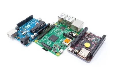
This article provides a comprehensive analysis of Arduino vs Raspberry Pi, highlighting their essentials, key features, and recent developments, helping you make an informed decision for your next project.
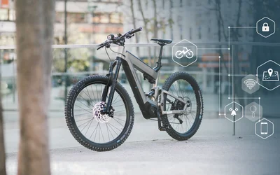
Take advantage of the low cost and high energy efficiency of SBCs to design your own tracking systems


How IoT devices and SBCs improve the quality of life and care for elderly people