What is a Multilayer PCB?
Multilayer PCBs are normal electrical boards that consist of two or more inner layers with a compact design, multiple functions, lightweight production, durability, and flexibility for a wide range of industries, including consumer electronics, telecommunications, defense and military, etc.

11 Jul, 2022. 9 minutes read
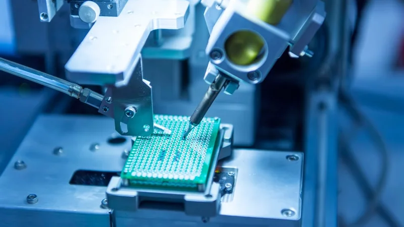
Manufacturing process of a multilayer PCB
Printed circuit boards are commonly seen in modern-day electronic and electrical appliances that are comprised of one or more insulating layers and copper layers. Planning the design of these multilayer PCBs is one of the important aspects to achieve a better electrical performance of the signal transmission. Poorly designed substrate and wrong choice of selected materials can degrade the performance to increase emissions and crosstalk to make it more susceptible to external noise.
A properly designed PCB board substrate can effectively reduce electromagnetic emissions, and crosstalk and also improve the signal integrity to provide low inductance power. The external noise needs to be suppressed at the source than trying to eliminate the noise once the product has been manufactured. This proper design of multilayer PCBs can increase immunity to RF fields by a factor of 10 or more, compared to the double-sided boards.
But overall, multilayer boards are expensive and harder to troubleshoot than any other simple double-sided printed circuit board. However, multilayer PCBs offer better shielding and signal routing, and there are more layout options for this kind of board design. In comparison to single or double-sided boards, multilayer PCBs provide extra density to route power and signal tracks. With this, the components can be packed tightly on the board to offer a more compact design.
Recommended reading: Rendering PCBs Part 1 - Preparation, Textures and UV Unwrapping
What is a multiplayer PCB?
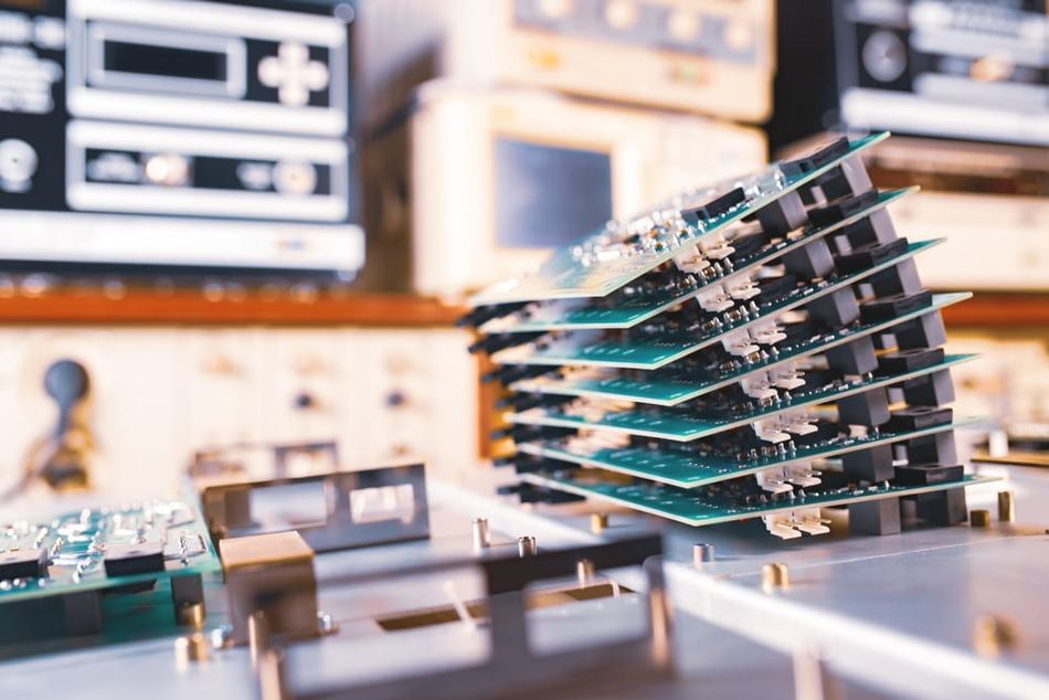
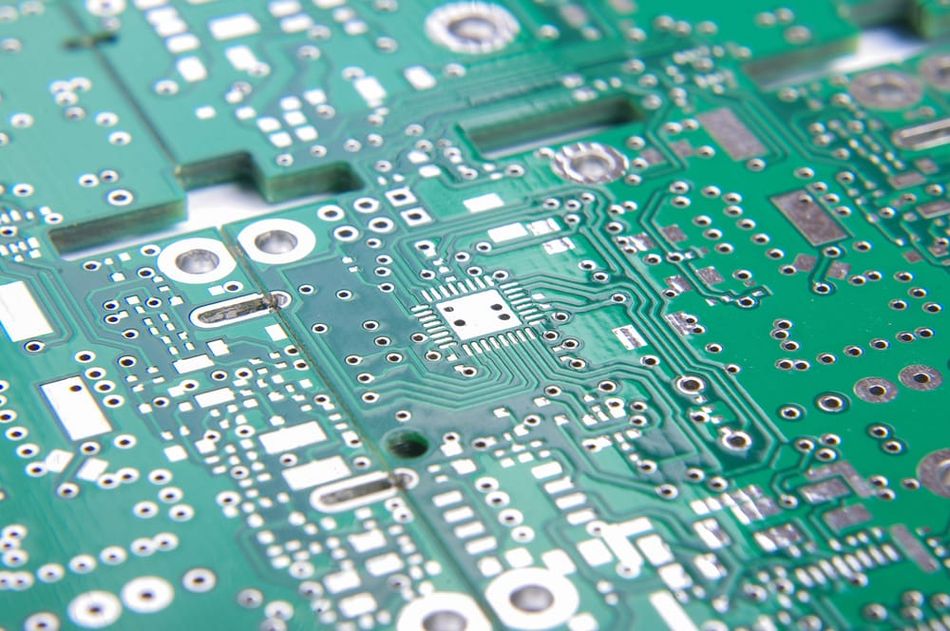
In simple words, Multilayer PCB is a printed circuit board with more than two layers and has a minimum of three conductive layers of conductive material or copper layer. When looking at a multilayer PCB, the top and bottom layers look similar to a double-sided PCB but they have more layers on both sides of the core. These layers are interconnected with copper-plated holes and there can be more layers as we have witnessed up to 40 layers. The active and passive components are placed on the top and bottom layers of the multilayer PCB while the inner stacked layers are used for routing.
As multilayer PCBs can accommodate more electronic components, they have been widely used in modern-day electrical appliances with variants ranging from four to twelve layers. Several applications, such as smart devices require between four to eight layers, while smartphones can use up to twelve layers. While manufacturing multilayer PCBs, designers choose an even number of layers over odd as laminating an odd number of layers can make the circuit complex and also result in high cost.
In a typical four-layer stack up, to improve the electromagnetic compatibility (EMI) performance, the signal layers should be spaced as close to the planes and use a large core between the power and ground plane. The tight coupling between signal trace and ground plane often reduces the plane impedance which further reduces the common-mode radiation from the cables connected to the printed circuit board. Also, the close trace to plane coupling will decrease the crosstalk between traces.
As we increase the number of layers to twelve, the high layer count boards require thin dielectric and hence they automatically have tight coupling between the layers. They are often used for high-speed electronics to deliver improved EMI performance and signal integrity. Interestingly, there is no limit to the number of layers that can be fabricated in a multilayer PCB. But as the layer increases, the board thickness also increases to accommodate the minimum thickness of materials used.
How do multilayer PCBs work?
The first step toward the multilayer PCB manufacturing process is to design the layout of the board using any of the PCB designing software, for example, Eagle, Proteus Altium, and KiCAD. Once the design is ready, it is important to make the inner layer core and laminate with desired thickness with copper foil, dry film resist and UV light. The next step in the design workflow is the lamination which includes the inner layer core, prepreg sheets, and copper foil sheets. Next is to apply pressure, heat and vacuum using a heated hydraulic press and it is important to make sure that there is no air trapped between layers. Once cured, resins from the prepregs join the sheets, core and foil to form a multilayer PCB.
In a multilayer PCB design, the designer needs to dedicate one layer to a ground plane and another to the power plane. For digital-only PCBs, the designer can also dedicate the entire power layer and if there is space on the top and bottom layer, that can be used to route any additional power rail tracks. The power layers are always in the middle of the board with the ground closer to the top layer. Once the power is taken care of on the inner layers, the remaining space is available for signal tracks that are routing. For example, in a six-layer stack up, there will be four signal routing layers and two layers dedicated to power.
Multilayer PCBs have two reference planes and a signal via. The signal via allows the electrical signal to flow through all the stacked planes which are used for routing. The stitching via is connected to one of the planes next to the signal via and provides a reduction in area for the signal flow. These types of PCBs have several different options of vias to improve the routing density– commonly referred to as standard, blind, and buried.
What is a PCB Via?
In simple words, via refers to an electrical connection between different layers on the printed circuit board. These are seen as small holes on the PCB that crosses two or more adjacent layers. Vias are different from plated through holes as they are used for electrical connection of through-hole components on the PCB and usually have larger dimensions than the vias. The via hole is covered with copper to form an electrical connection in the insulating material that separates the different layers of the printed circuit board. Depending on the application requirements, the board may require vias that cross all the layers of the stock or only one of the outermost layers. As mentioned earlier, there are three types of vias– standard (also referred to as through-hole via), blind, and buried.
Through-hole Via
The standard vias are seen to pass all the layers of the printed circuit board to connect the top, bottom and inner layers. They have large dimensions than the other types of vias and are simpler to make as there is no restriction on the drilling process.
Blind Via
The blind vias typical are drilled from the outside layer of the printed circuit board to the inner layers and do not make a hole on the other side of the board. They are referred to as ‘blind’ because the hole cannot be seen from another side of the board. In the case of multilayer boards, these types of vias can introduce challenges to manufacturing as the designer needs to precisely determine when to stop the drilling process to achieve the desired degree of depth. They are used for increasing the number of connections between the outer and inner layers of the printed circuit board.
Buried Via
The buried vias are used to connect two or more inner layers of the printed circuit board and hence are not visible on either outer layer. In the case of multilayer PCBs, the internal plating of the buried vias must be completed before applying the two outer layers of the board. Buried vias can increase the manufacturing cost as it requires more precision to design.
Recommended reading: Rapid PCB Prototyping with Cloud Manufacturing
Advantages of Multilayer PCBs
Even though the design process for multilayer PCB is complex and requires domain expertise, they possess several benefits that make them widely used in modern-day advanced electronic devices and electrical appliances. Here are some of the benefits of multilayer printed circuit boards:
Reduced form factor: Multilayer PCBs have used evolving manufacturing processing and advanced design rules to reduce the size of the boards with maintaining the same functionalities. Multilayer PCBs are also used in smartphones and electronic gadgets that require small size, and hence they are easily adapted for the growing demand for electronic wearables.
Advanced manufacturing techniques to result in lightweight boards: These multilayer printed circuit boards are manufactured to achieve less weight and can be used in wearable smart devices. One of the highlighted reasons for the reduction in weight is the elimination of multiple connectors required to interlink separate double-sided PCBs of a multilayered design.
Production of multifunctionality board with high quality: There is a tremendous amount of work done in the design and manufacturing process to offer multifunctionality in the small form factor printed circuit board. To be used in smartphones, they possess several functionalities which are usually not offered by a single-layer board due to its limitations.
More durability and flexibility for long-term use: This kind of printed circuit board is designed to withstand more weight and is also able to handle the heat and pressure used to bind the layers together. Also, they provide flexibility to be tweaked according to the applications and do not require a complete re-design.
Single connection point: Multilayer PCBs are designed to work on a single connection point than the multiple connection points required to use multiple single-layer PCBs.
Disadvantages of Multilayer PCBs
Even though there are many benefits of using multilayer PCBs, you should also be aware of the downsides of the manufacturing and designing process. Here is a list of disadvantages of multilayer PCBs:
Elevated cost of production: Multilayer PCBs are more expensive than single and double-sided PCBs at every stage of the manufacturing process. There is an increased amount of labour work and advanced design along with the pricey assembly machinery.
Complex design process: It takes an increased amount of hours for designing multilayer PCBs and also the designer needs to follow many design rules. The choice of lamination and substrate also depends on the type of applications and the number of active and passive components to be mounted.
Required domain expertise: Multilayer PCBs cannot be designed by anyone as they require experience in CAD tools and an understanding of design rule checks. Due to several challenges in the design process, domain expertise is essential.
Recommended reading: Engineer's Guide to PCB Manufacturing and Intellectual Property
Multilayer PCB Applications

Modern-day consumer electronic appliances: As we have mentioned earlier, smartphones and smart devices use multilayer PCBs due to their small form factor and multifunctionality.
Telecommunication industry: Network appliances and transmission devices use multilayer PCBs due to their durability and flexibility to adapt to outdoor and indoor environments.
Manufacturing industry and production line: With its durability comes the capability to be used in extreme industrial setups to withstand pressure, heat, and high temperature. Also, the multifunctionality and small form factor are other reasons for its extended adoption.
Medical devices and the healthcare industry: Medical equipments require precise functioning for treatment and diagnosis. Multilayer PCBs are used in the medical industry due to their less weight and extensive robust functionalities.
Military and defense: Durability and low weight are essential factors to be used in military and defense. Multilayer PCBs provide compact designs with small size boards for more room for other components and custom functionalities.
Automotive and aerospace systems: These industries are dependent on precision and extreme conditions. Multilayer PCBs can withstand extreme operating conditions and do not damage the product to maintain its quality and functionality.
Key Takeaways
Multilayer PCBs are normal electrical boards that consist of two or more inner layers to the outermost layers considered as power and ground plane.
Designing multilayer PCBs is a complex task and requires domain expertise to achieve improved electrical performance and reduce external noise.
With high production costs comes the multifunctionality features, and this is the trade-off designers should be aware of.
There are several advantages to the production of multilayer PCBs, including small form factor, multiple functions, lightweight production, durability, and flexibility.
There are a few downsides as well, which are the elevated cost of production, requiring domain expertise to design the boards, and a complex design and manufacturing process.
The multilayer boards are used across a wide range of industries, including consumer electronics, telecommunications, defense and military, etc.
References
[1] Available online: https://resources.altium.com/sites/default/files/uberflip_docs/file_738.pdf; Accessed. July 8, 2022.
[2] Available online: https://smtnet.com/library/files/upload/Multilayer-PCB-Stackup.pdf; Accessed. July 8, 2022.
[3] Available online: http://www.idc-online.com/technical_references/pdfs/data_communications/Multilayer_PCB.pdf; Accessed. July 8, 2022.
[4] Available online: https://www.oki.com/en/otr/2010/n216/pdf/otr-216-R07.pdf; Accessed. July 9, 2022.
[5] Available online: https://narasimmamohan.files.wordpress.com/2019/09/design-of-multilayer-pcbs-smd-mounting-techniques.pdf; Accessed. July 10, 2022.
[6] Available online: https://www.analog.com/media/en/training-seminars/design-handbooks/Basic-Linear-Design/Chapter12.pdf; Accessed. July 10, 2022.
[7] Available online: https://server.ibfriedrich.com/wiki/ibfwikien/images/d/da/PCB_Layout_Tutorial_e.pdf; Accessed. July 10, 2022.