Sputtered TFLN (Thin Film Lithium Niobate) as a Cost-Effective Option for High-Performance Photonics
TFLN offers a much smaller footprint and improved modulation efficiency, making it highly attractive for short-reach optical communication and future integrated photonics.

30 Jun, 2025. 6 minutes read
Lithium Niobate (LiNbO₃) has long been a foundational material for high-speed optical modulators due to its strong electro-optic effect, broad optical transparency, and excellent thermal stability. The first generation of optical modulators, based on bulk lithium niobate (LN), has been widely adopted in long-haul optical communication networks, where the high cost and large form factor were acceptable due to the limited deployment volumes. However, bulk-LN modulators are too large and power-hungry for chip-scale integration, prompting the development of thin-film lithium niobate (TFLN) devices as a second-generation solution. TFLN offers a much smaller footprint and improved modulation efficiency, making it highly attractive for short-reach optical communication and future integrated photonics.
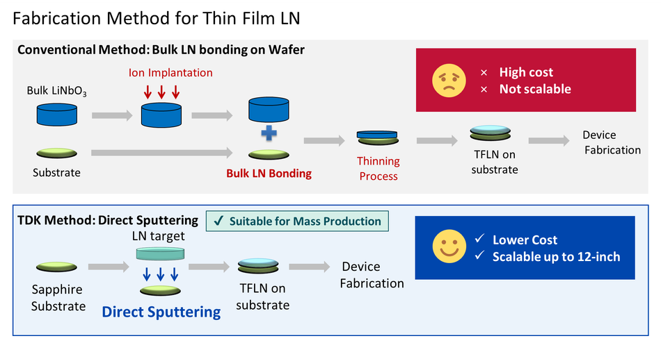
Despite being labeled “thin-film,” most commercial TFLN today is produced by bonding bulk-LN crystals onto silicon or other wafers and then mechanically thinning them down to form films. This bonding-based process inherits many of the same drawbacks as bulk-LN, including high cost, low yield, and poor compatibility with mass-production semiconductor workflows. Moreover, while TFLN has gained momentum in recent years, only a few top-tier companies have released early commercial products, and the technology remains largely in the pre-volume development phase.
TDK has introduced a third-generation approach by eliminating bulk bonding altogether. Instead, TDK forms TFLN directly through sputtering: a physical vapor deposition method that deposits LN films onto wafers using standard semiconductor processes. With this advancement, TDK is enabling chip-scale photonic integration without sacrificing the performance characteristics lithium niobate is known for. By offering a high-quality, scalable, and CMOS-compatible method of deposition, sputtered TFLN unlocks new potential in optical communications, on-chip optical interconnects for AI systems, and next-generation imaging devices for AR smart glasses.
The Limitations of Bulk-LN Bonding
Despite the exceptional electro-optic properties of LN, its current fabrication method of bulk bonding for TFLN presents significant limitations for modern photonic applications.
Bulk-LN bonding involves mechanically attaching a thick lithium niobate crystal to a separate wafer substrate, followed by a thinning process of the bonded material to form a thin film. This process is labor-intensive and requires extreme precision to ensure uniform thickness and surface quality, both of which are critical for consistent optical performance.
One of the most significant drawbacks of TFLN by bulk-LN bonding is its incompatibility with semiconductor industry standards. The mechanical nature of the bonding process introduces alignment variability, poor yield, and high defect rates when scaling down to chip-sized devices. These factors severely limit the integration of photonic integrated circuits (PICs), each of which requires tight dimensional tolerances and lithographically defined architectures. As a result, while TFLN by bulk-LN bonding can be used for long-haul telecom infrastructure, it falls short when applied to large-number-required data center applications or optical interconnects for GPUs and/or HBM.
From a cost perspective, the bulk bonding approach is neither cost-effective nor scalable for large volume production. High-quality single-crystal LN is expensive to produce, and the wafer bonding and thinning steps require costly equipment and process control. The need for specialized infrastructure further complicates the fabrication pipeline and reduces throughput. For optical modulators operating at high speed, this results in devices that are too costly for widespread deployment in consumer electronics or AI infrastructure.
For scalability, the batch size for bonded wafers is small, and yield losses further reduce output efficiency. It therefore becomes challenging to produce thousands or millions of devices per month at competitive price points compared to conventional semiconductor processes.
In short, while TFLN by bulk-LN bonding remains suitable for low-volume and performance-driven markets, it is fundamentally misaligned with the demands of modern high-volume photonic manufacturing. To enable chip-scale optical devices with broad commercial applicability, a new approach for the preparation of TFLN integration is needed.
Sputtered TFLN (Thin Film Lithium Niobate)
TDK’s innovation in sputtered TFLN addresses the central limitations of traditional bulk bonding TFLN by reimagining how LN can be integrated into photonic devices. Rather than bonding a bulk crystal onto a separate wafer and thinning it, TDK employs a thin-film sputtering process to directly deposit TFLN onto the substrate. Importantly, this method aligns with established semiconductor manufacturing techniques and opens the door to scalable, high-throughput production of optical components at the wafer level.
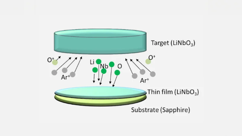
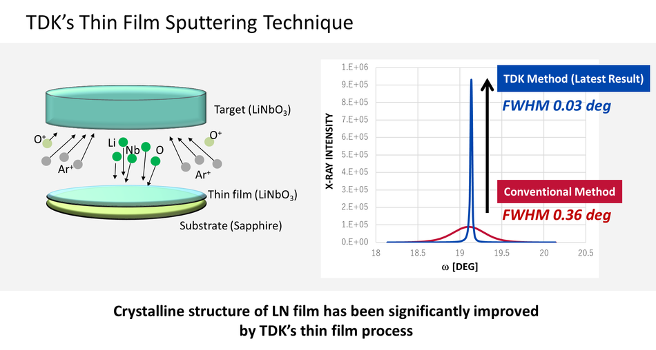
Sputtering is a physical vapor deposition (PVD) technique in which energetic ions (e.g., typically argon) are directed at a LN target, dislodging atoms that then condense onto a substrate to form a thin film. By carefully controlling sputtering parameters such as ion energy, pressure, substrate temperature, and partial oxygen gas pressure, TDK achieves uniform crystalline films with optical quality suitable for high-speed modulation. These films are deposited directly on sapphire wafers, which serve as stable platforms for subsequent processing steps such as etching, electrode deposition, and waveguide formation.
This shift from mechanical bonding to thin-film sputtering provides advantages with respect to manufacturing scalability and cost reduction.
First, sputtering eliminates the complex alignment and post-processing steps required in bonded LN for a more reliable, repeatable, and automation-friendly workflow. Second, it enables batch processing on full wafers (i.e., even up to 12 inches in diameter) using existing semiconductor production equipment. With this infrastructure already in place across fabs worldwide, TFLN-based devices can now be produced at scale using familiar tools and cleanroom practices.
And, by removing the need for bulk crystal handling and alignment, sputtered TFLN fabrication dramatically reduces material waste and process variability. In turn, this lowers the per-unit cost of photonic components and significantly improves yield. The technology is also well-suited for high-density optical interconnects in artificial intelligence (AI) and data center systems that require cost-efficient deployment of photonic links for scaling bandwidth without increasing power consumption.
Beyond cost, sputtered TFLN also reduces production time. Without the need for mechanical bonding and thinning processes, cycle times shrink, iteration is faster, and development timelines shorten.
TDK’s sputtered TFLN also demonstrates strong crystalline quality, as confirmed by X-ray diffraction and full-width half-maximum (FWHM) measurements. The films maintain the electro-optic and optical transparency characteristics necessary for device-grade performance. This breakthrough solidifies sputtered TFLN as a truly superior alternative to bonded wafers that does not compromise quality.
Future Application of Sputtered TFLN
Today’s computing architectures are rapidly evolving to meet the bandwidth and energy demands of modern, data-intensive workloads. Given all of its benefits, sputtered TFLN is now a compelling solution for next-generation optical communication and/or optical interconnects, such as GPU to other semiconductor chip interconnects.
In co-packaged optics (CPO) and optical interposers, for example, optical engines are integrated near semiconductor chips. Here, traditional electro-optic materials in silicon photonics struggle to achieve high-speed modulation and a wide bandwidth. Sputtered TFLN, by contrast, can achieve higher-speed modulation and much wider bandwidth than silicon photonics. The result is low-latency, high-density optical links.
For generative AI workloads, which increasingly rely on massive data flow between processors, GPUs, and HBM, the I/O bottleneck has become a bottleneck. Optical interconnects offer a path to scale bandwidth without the energy penalties of electrical signaling, and TFLN modulators enable compact, low-power, high-speed solutions compatible with CMOS manufacturing. By supporting higher modulation speeds per channel and operating efficiently across temperature ranges, sputtered TFLN makes it feasible to deploy optical interfaces between racks and between chips within advanced packaging substrates.
The thin-film form factor also allows for advanced photonic integration. For example, photonic integrated circuits (PICs) based on sputtered TFLN can include waveguides, multiplexers, and modulators on a single chip. Sputtered TFLN functionally reduces the need for discrete components and thereby minimizes parasitics associated with layouts.
Conclusion
Sputtered TFLN is a true paradigm shift in the integration of lithium niobate for high-performance optics. In place of traditional bulk bonding methods, which are costly, size-constrained, and incompatible with semiconductor workflows, sputtering enables direct thin-film deposition using standard fabrication tools to dramatically reduce cost, eliminate post-processing steps, and make mass production feasible for the first time.
TDK’s pioneering work in this domain preserves the exceptional electro-optic properties of TFLN and unlocks its potential for scalable use in optical communications, optical interconnects for AI-driven data infrastructure, and AR smart glasses. As the industry moves toward integrated optical I/O and chip-scale photonics, TDK invites system architects and chipmakers to collaborate in deploying sputtered TFLN in real-world platforms.
To learn more, get in touch with TDK here.
References
Fukuzawa, H., et al. (2022). Visible light modulator by sputter-deposited lithium niobate
Visible light red, green, and blue multiplexer by sputter-deposited thin-film lithium niobate
TDK develops world’s first full-color laser control device for 4K smart glasses
Envisioning the Future of AR Glasses Through TDK’s Augmented Reality Solutions