Leveraging JFETs in Piezoelectric and Pyroelectric Sensor Applications
This paper explores why JFETs continue to be the interface of choice for high-impedance sensor design where fidelity and low noise are paramount.

30 Jun, 2025. 8 minutes read

Piezoelectric and pyroelectric sensors are widely deployed in systems where mechanical or thermal energy must be transduced into an electrical signal. In aerospace, defense, medical diagnostics, and industrial monitoring, these sensors enable detection of dynamic pressure changes, vibration, thermal events, or mechanical displacement with high temporal resolution. Still, despite their versatility, these devices pose significant interfacing challenges at the circuit level.
Fundamentally, piezoelectric and pyroelectric transducers behave as charge generators in parallel with extremely high output impedance and modest intrinsic capacitance. Source impedances often exceed hundreds of megohms and can approach or surpass one gigaohm. Notably, the signals generated are typically low in amplitude, often in the sub-microvolt range, and can be distorted or lost entirely in the presence of input bias currents or noise. These characteristics necessitate an interface circuit that offers ultra-high input resistance, negligible gate leakage, and minimal input-referred noise current.
The junction field effect transistor (JFET) satisfies these requirements in a way unmatched by either bipolar junction transistors or MOSFETs. Operating as a depletion-mode device with a reverse biased gate channel junction, the JFET naturally achieves sub picoampere gate currents, input resistance in the teraohm range, and low input capacitance. Equally important, its noise characteristics enable faithful extraction of weak signals without corrupting signal-to-noise ratio or introducing low frequency drift.
This paper explores why JFETs continue to be the interface of choice for high-impedance sensor design where fidelity and low noise are paramount.
Piezoelectric and Pyroelectric Sensor Fundamentals
Piezoelectric and pyroelectric sensors exploit material properties that convert physical stimuli into electrical charge. In piezoelectric materials, mechanical stress, such as vibration or strain, displaces charge centers within the crystal lattice and induces a net surface charge. Pyroelectric materials, by contrast, generate charge in response to changes in temperature due to a shift in spontaneous polarization. In both cases, the output signal is a flow of charge, often on the order of femtocoulombs to picocoulombs, rather than a sustained voltage or current source.
Electrically, these sensors are modeled as ideal charge sources in parallel with a capacitive element representing the dielectric behavior of the material and a very large leakage resistance.
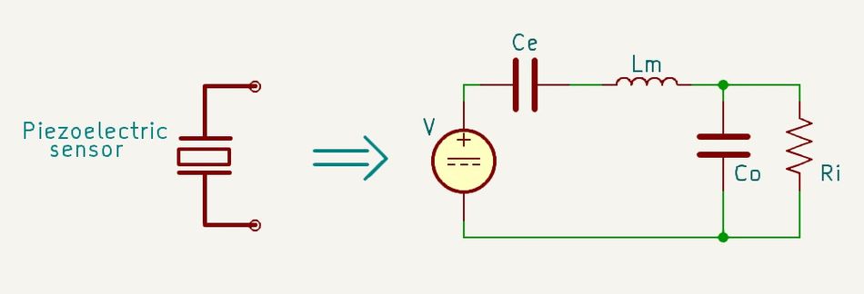
Typical values for capacitance range from a few picofarads to several nanofarads, while leakage resistance may exceed hundreds of megohms or even reach into the gigaohm range. This combination defines a high impedance, charge generating node that is highly sensitive to circuit loading, parasitic capacitance, and input current noise.
Because of this, interfacing circuits must offer ultra-high input resistance and negligible gate or bias current to avoid draining or corrupting the generated signal. Even nanoamp level currents can rapidly discharge the signal carrying capacitance and cause baseline drift or total loss of low frequency information. Input capacitance must also be minimized to preserve bandwidth and maintain a fast response.
Depending on the source impedance and signal frequency content, either voltage mode or charge mode amplification is appropriate. Charge amplifiers are preferred when the source impedance is high and the frequency content is low, as they establish a defined gain independent of sensor capacitance. In contrast, voltage mode amplifiers may be used when the sensor’s output impedance is relatively low, and the design can tolerate bandwidth limitations due to input capacitance.
Why JFETs? Device Structure and Electrical Advantages
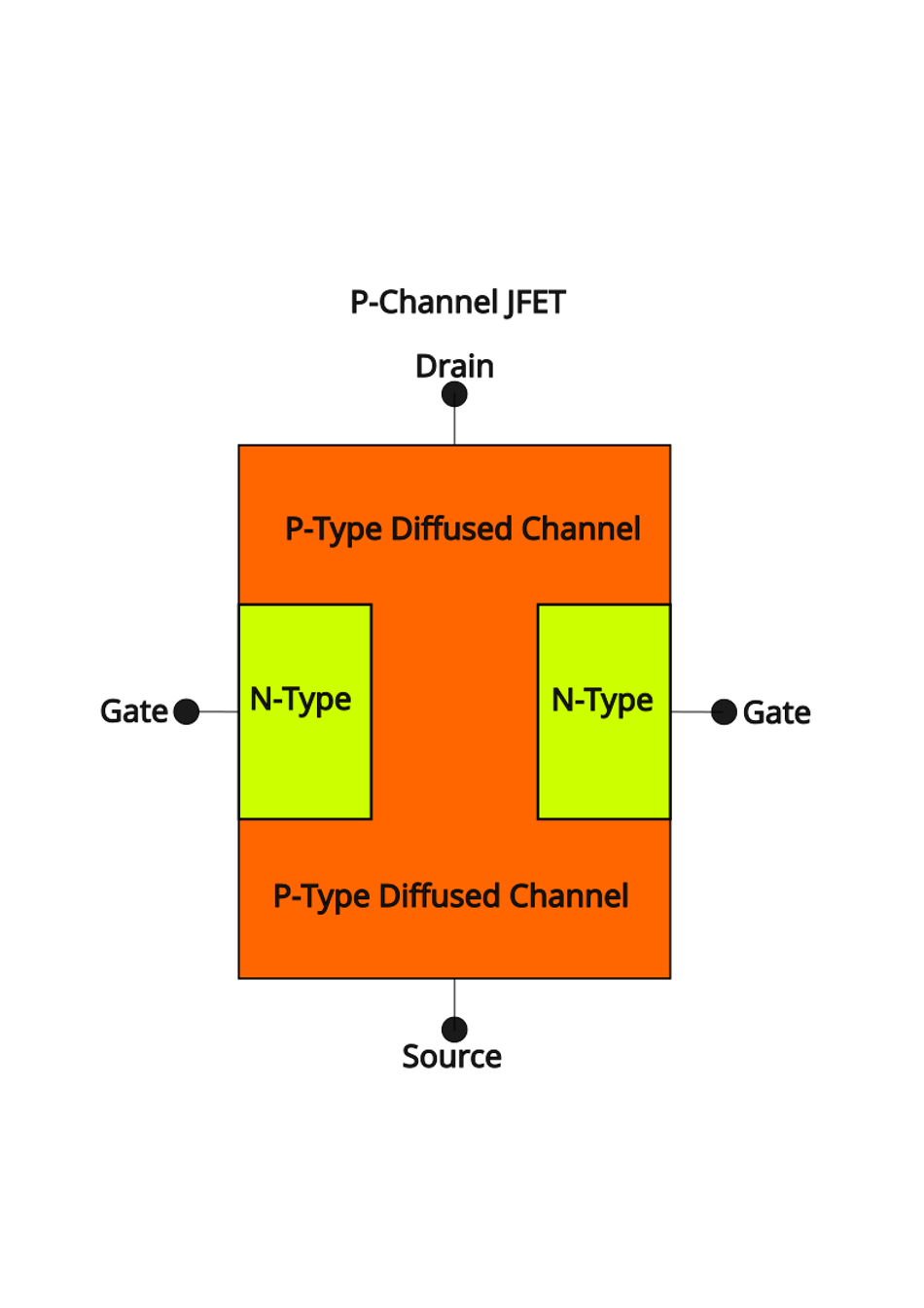
The JFET is fundamentally a depletion-mode, majority carrier device. Its construction consists of an n-type (or p-type) semiconductor channel with ohmic source and drain terminals, flanked laterally by a reverse biased p-n junction gate. When a negative gate-source voltage is applied (for an n-channel device), the depletion region expands into the conductive channel, constricting electron flow and reducing drain current. Crucially, since the gate junction remains reverse biased under normal operation, the steady-state gate current is negligible (i.e., typically in the sub-picoampere range), yielding input resistances on the order of teraohms.
This structure inherently favors high-impedance signal acquisition. Whereas bipolar junction transistors rely on forward biased base-emitter junctions and draw finite base current even in the nanoampere range, JFETs impose virtually no load on the signal source. Compared to MOSFETs, which also offer high input resistance, JFETs benefit from the absence of a gate oxide and are less susceptible to long-term drift caused by charge trapping, gate leakage due to dielectric breakdown, or electrostatic discharge.
Otherwise, important performance metrics for JFETs in sensor interfacing include high transconductance (typically tens of mS), low gate-to-source capacitance (2–5 pF), and minimal gate leakage currents (<1 pA at room temperature). These characteristics remain relatively stable across drain current and gate bias operating points, offering predictable performance and design flexibility.
In contrast, bipolar devices exhibit increasing input noise current at low collector currents, while MOSFETs experience non-negligible oxide-related leakage and higher flicker noise below 100 Hz. For these reasons, the JFET remains the preferred active device in charge amplification circuits.
JFET-Based Charge Amplifier Architectures
Interfacing piezoelectric and pyroelectric sensors requires a front-end circuit that maintains the sensor’s high-impedance characteristics while accurately extracting the generated charge. JFETs, due to their exceptionally low gate current and high input resistance, form the core of multiple suitable amplifier configurations.
Basic Source Follower
A single JFET source follower is the simplest topology used in high-impedance buffering. Here, the gate is connected to the sensor output, and the source is biased through a resistor to a defined voltage, typically ground. This self biased configuration provides input impedances exceeding 1 GΩ, limited primarily by the gate leakage current and gate-bias resistor value. Because the JFET gate draws negligible current, the sensor retains its charge long enough for downstream processing without significant discharge.
In AC coupled applications, a series capacitor may be introduced between the sensor and gate to block DC offset. However, the parasitic capacitance of the JFET, generally gate to drain capacitance, can interact with the source impedance and load and affect the frequency response. To maintain signal integrity and low-frequency gain, the bias resistor must be carefully chosen to avoid excessive corner frequency shift while maintaining thermal noise within limits.
Differential Source Followers
In environments with temperature gradients or mechanical noise, offset voltages and drift can degrade low frequency accuracy. For such applications demanding greater stability and common mode noise rejection, a matched dual JFET differential source follower is often preferred. In this topology, two JFETs form the input stage of a balanced amplifier, where the symmetry enables suppression of temperature induced parameter drift and improves the common mode rejection ratio (CMRR).
To maintain balance, both JFETs must be closely matched in terms of transconductance, threshold voltage, and leakage characteristics. Integrated dual JFET dies are often used to guarantee thermal tracking and parameter symmetry, although discrete hand matching is sometimes employed in low volume builds. The differential configuration enhances linearity and minimizes output offset caused by parameter variation.
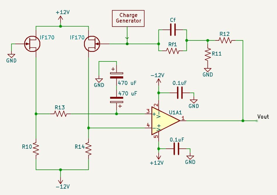
Charge Amplifier Topologies
The canonical charge amplifier employs a JFET in an inverting amplifier configuration with a feedback capacitor CF and a large valued feedback resistor RF. The sensor is connected directly to the gate node, and the JFET converts the incoming charge Qto an output voltage via the relation

This gain is independent of the sensor capacitance Csensor , which is critical for maintaining consistent signal levels across varying operating conditions or sensor tolerances. The resistor RF sets the low-frequency cutoff and determines the response to slow changing or static inputs.
Practical Design Considerations
Stability in charge amplifier configurations hinges on the appropriate selection of the feedback network. Excessively large feedback resistors may introduce time constants in the range of several seconds, resulting in drift or delayed baseline recovery. Too small values compromise the charge retention advantage. Moreover, parasitic capacitance and layout stray inductance can lead to peaking or oscillation unless compensated with phase margin adjustments via the addition of a small compensation capacitor across the feedback path or using series damping resistors.
Maintaining sufficient phase margin (>45°) requires modeling the sensor, layout, and feedback loop as a distributed system, especially when the signal chain includes cable capacitance or remote sensors.
JFET Noise Performance in High-Impedance Designs
When interfacing sensors with extremely high source impedance, amplifier input noise becomes a limiting factor in overall system resolution. For such systems, JFETs offer a fundamental noise advantage due to their low gate current and dominant thermal noise characteristics.
Quantitatively, JFETs achieve input voltage noise densities as low as 1–5 nV/√Hz in the 1 kHz region, with corresponding input current noise densities of less than 10 fA/√Hz. By contrast, bipolar input stages at collector currents below 100 μA can exhibit input current noise in the range of 0.3 to 1 pA/√Hz, which becomes unacceptable for source resistances above 1 MΩ. When the input current noise is multiplied by the source resistance, the resulting voltage noise contribution often dominates the system noise. In JFETs, this term is negligible even for gigaohm-scale source resistance, resulting in total noise figures well below 1 dB for source impedances up to 1 GΩ.
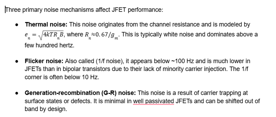
In high impedance pyroelectric circuits, gate leakage and junction capacitance introduce long-term drift and settling time issues if not tightly controlled. JFETs exhibit leakage currents below 1 pA at room temperature and gate to source capacitance in the range of 2–5 pF that allow the sensor to retain its generated charge over extended durations without baseline decay. This behavior contrasts sharply with MOS devices, where gate oxide leakage and charge trapping degrade long-term stability.
Practical Design Considerations
Designing high fidelity front ends for piezoelectric and pyroelectric sensors requires careful attention to biasing, linearity, and bandwidth control to ensure consistent performance across temperature, time, and frequency.
Biasing techniques are central to achieving stable DC operation. JFETs typically operate in the saturation region with gate-source voltage near 0 V. Self biasing through a source resistor provides thermal stability by introducing negative feedback: as temperature rises and drain current increases, the resulting source voltage reduces gate-source voltage and effectively compensates for drift. In more precision sensitive applications, constant current biasing or active bias control circuits are used to maintain a fixed drain current and guarantee consistent transconductance and noise behavior across varying ambient conditions.
Device matching is also needed in differential configurations. Matched dual JFETs with tightly controlled parameters, like threshold voltage and transconductance, minimize offset voltage and thermal drift. Such features are needed where gain stability is required across temperature or when long-term calibration integrity is a concern.
To mitigate intermodulation distortion, designs must minimize nonlinear parasitic effects such as voltage dependent capacitance between gate and drain (Crss). Low Crss JFETs reduce Miller capacitance effects and help preserve linearity. Cascoding techniques, in which a second transistor holds the drain at a fixed potential, can effectively eliminate drain-gate voltage modulation, thereby flattening the JFET's voltage gain and minimizing signal induced distortion.
Finally, bandwidth extension can be achieved through resistive equalization and segmentation. For instance, dividing high value feedback resistors into multiple smaller segments reduces parasitic capacitance per segment, improving phase margin and preserving high frequency gain. Alternatively, adding a small resistor in series with the gate can dampen resonances caused by cable or trace inductance without compromising input impedance.
Conclusion
Junction field-effect transistors remain the gold standard for interfacing high impedance charge generating sensors such as piezoelectric and pyroelectric devices. Their intrinsic properties allow them to interface with source impedances that would overwhelm bipolar or CMOS-based front-ends. Unlike bipolar junction transistors, which suffer from excessive shot noise at low bias currents, or MOSFETs, which are vulnerable to charge trapping and gate oxide degradation, JFETs deliver stable, low-noise performance across time, temperature, and frequency.