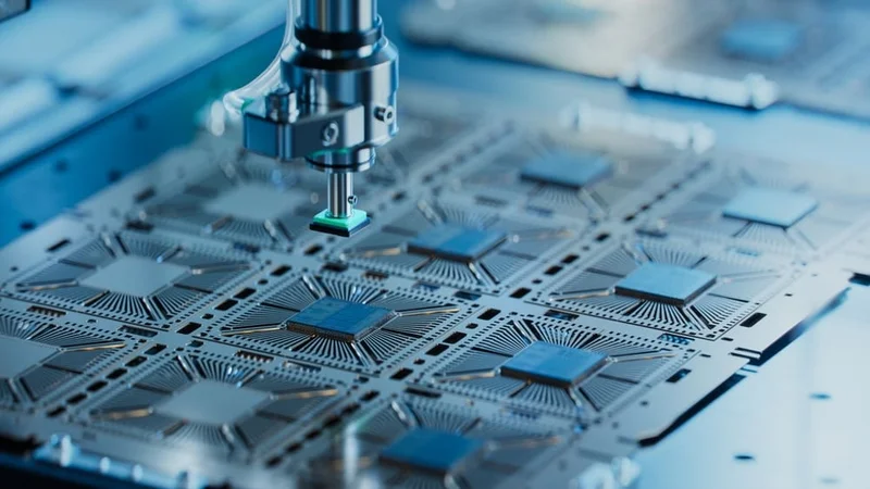
Die Attach: A Comprehensive Guide
Die attach, also known as die bonding or die mount, is a process used in the semiconductor industry to attach a silicon chip to the die pad of a semiconductor package's support structure, such as a leadframe or metal can header. This article explores the fundamentals of die attach, its importance, materials, and methods used in die attach, its parameters, quality, and reliability techniques.

31 May, 2023. 18 minutes read
Die attach (semiconductor packaging)
Introduction
The term "die attach" describes a crucial step in the construction and packaging of semiconductor devices. It's a technique for joining the semiconductor die—the brains—to the substrate or package. According to the layout and function of the electronic device, these packages can take on a variety of shapes, such as lead frames, ceramic substrates, or printed circuit boards (PCB).
The die attach procedure is essential to the functionality and reliability of electronic equipment. It shields the sensitive die from physical pressures and shock by forging a solid mechanical bond between the die and the package. Additionally, the die connects layer functions as a thermal bridge, making it possible for heat to be efficiently transferred from the die to the package or substrate. This is essential for keeping the operating temperature within safe ranges. For high-power devices, where excessive heat might result in performance degradation or device failure, this thermal management component is particularly crucial.
Common materials used for die attachment, commonly called die bonders, include solder alloys, conductive adhesives, and eutectic compounds. These materials are chosen based on various factors such as their mechanical strength, thermal conductivity, electrical conductivity, and compatibility with the die and substrate materials. The specific choice of die attach material can significantly impact the performance and longevity of the electronic device.[1]
Fundamentals of Die Attach
The term "die" is used to describe the tiny piece of semiconducting material on which a working circuit is constructed in the field of microelectronics. Typically, silicon is used to make the die, although depending on the application, gallium arsenide or silicon carbide may also be employed. The die, which contains the transistors, capacitors, and resistors that make up electrical circuits, is where the magic of electronics happens.
The die attach process ensures that the die is securely connected to the package or substrate. This connection serves two main purposes. First, it provides a stable mechanical linkage, securing the die in place to withstand the physical stresses associated with handling, assembly, and use of the electronic device. Second, it establishes a thermal pathway, allowing heat generated by the die during operation to be conducted away to the package or substrate, from where it can be further dissipated to the surrounding environment.
The choice of materials used in die attachment is a critical aspect of the process. These materials, often referred to as "die attach materials" or "DAMs", must satisfy a range of requirements. They need to have high mechanical strength to securely hold the die in place, and high thermal conductivity to efficiently transport heat away from the die. They should also have good electrical characteristics, since in some designs, the die attach layer also serves as an electrical connection between the die and the package.
A variety of materials can be used as DAMs, including metal alloys, ceramics, and polymers. Metal alloys, such as gold-tin or gold-silicon eutectic alloys, are often used due to their high thermal and electrical conductivity. However, they require high processing temperatures and can be expensive. Ceramic materials, such as silver-filled glass, are also used, offering a good balance between thermal performance, electrical isolation, and cost. Polymers like epoxy resins filled with silver particles are another popular choice, especially for lower-cost applications. They are easy to process and can provide good mechanical strength and thermal performance.[2]
Importance of Die Attach
The importance of the die attach process cannot be overstated. It's a key determinant of the overall performance and reliability of the electronic device.
One critical role of die attach is thermal management. In operation, the electronic circuits on the die generate heat. If this heat is not efficiently conducted away, it can cause the die's temperature to rise significantly, affecting the performance of the electronic circuits and potentially leading to device failure. The die attach layer serves as a crucial thermal pathway, conducting heat from the die to the package or substrate. For instance, a gold-silicon eutectic alloy used as a DAM has a thermal conductivity of around 57 W/mK, allowing it to efficiently transport heat away from the die.
Die attach also contributes to the mechanical stability of the device. The die is fragile, and physical stresses—whether from the assembly process, mechanical shock during handling or use, or thermal expansion and contraction—can cause it to crack or delaminate from the package. A good die attach process creates a strong mechanical bond between the die and the package, helping to protect the die from these stresses.
Furthermore, the die attach process impacts device reliability. Imperfections in the die attach layers, such as voids or non-uniformities, can lead to localized hot spots on the die or uneven mechanical stresses, potentially causing device failure over time. A high-quality die attach process is therefore essential to ensure long-term device reliability. For instance, a study on epoxy-based DAMs found that reducing void content to less than 1% could significantly enhance the lifetime of power electronic devices.[3]
Materials Used in Die Attach
In the world of die attach, a multitude of materials are used, each with its unique set of properties that make it more suitable for certain applications over others. These materials are primarily categorized into three types: metal alloys, ceramics, and polymers.
Metal alloys are favored for their high thermal and electrical conductivity. For instance, gold-tin (AuSn) is one of the most commonly used metal alloy for die attach. It has a melting point of 280°C and a high thermal conductivity of 58 W/mK. This makes it an excellent choice for high-power devices where efficient heat dissipation is critical. However, the high cost of gold makes this option less attractive for cost-sensitive applications.
Another commonly used metal alloy is gold-silicon (AuSi). This eutectic alloy has a melting point of 363°C, higher than that of AuSn, making it suitable for devices operating at higher temperatures. AuSi also has a high thermal conductivity, around 57 W/mK, making it a solid choice for thermal management.
Ceramic materials, specifically silver-filled glass compounds, are also employed in die attach. These ceramics balance thermal performance, electrical isolation, and cost. For instance, silver-filled glass compounds can achieve thermal conductivities in the range of 3-4 W/mK. While significantly lower than metal alloys, this is sufficient for many applications. Additionally, these materials can be processed at lower temperatures compared to metal alloys, typically around 200°C, making them compatible with temperature-sensitive devices.
Polymers, particularly silver-filled epoxy resins, are used extensively in die attach, especially in lower-cost applications. Silver particles are mixed into the epoxy resin to improve its thermal conductivity. While a pure epoxy resin might have a thermal conductivity of just 0.2 W/mK, the addition of silver particles can increase this to 3-4 W/mK, comparable to silver-filled glass ceramics. Furthermore, these polymer-based DAMs can be processed at low temperatures, typically below 150°C, and they can also provide good mechanical strength to hold the die securely in place.
All these materials contribute significantly to the overall performance and reliability of the electronic device. The choice of the appropriate die attach material is dependent on many factors including the operating conditions of the device, the thermal and electrical requirements, and the cost considerations.[4]
Die Attach Methods
When discussing die attach methods, the field is often divided into two major categories: eutectic and adhesive die attach. These methodologies differ in terms of the materials used, the processing conditions, and the resulting characteristics of the die attach.
Eutectic Die Attach
Eutectic die attach, as the name suggests, leverages eutectic alloys in the die bonding process. A eutectic alloy is a specific mixture of metals that has a unique property: it melts at a lower temperature than any other mixture of the same metals. This characteristic makes eutectic alloys highly valuable in die attach, as it allows for high-quality bonding at relatively low processing temperatures. In fact, advanced eutectic packaging is continuing to adopt complete automation faster due to the rising demand for high-volume manufacturing.
The most common eutectic alloy used in die attach is the gold-tin (AuSn) alloy, mentioned earlier. With a melting point of 280°C, it provides a strong, reliable bond without requiring excessively high temperatures that could potentially damage the die or the substrate.
Eutectic die attach is generally performed in a two-step process. First, the eutectic alloy is deposited onto the die or substrate, often by a process such as electroplating or sputtering. This forms what is known as the "preform". Next, the die is placed onto the preform, and the assembly is heated to the melting point of the alloy. This causes the alloy to reflow, spreading out to cover the entire interface between the die and the substrate. Once cooled, the alloy solidifies, creating a robust bond between the die and the substrate.
This method is highly regarded for its excellent thermal and electrical conductivity. This is due to the nature of the materials used. Metal alloys like AuSn have significantly higher thermal and electrical conductivities than the polymers used in adhesive die attach. Thus, eutectic die attach is often the preferred choice for high-power or high-frequency devices, where efficient heat dissipation and minimal electrical resistance are critical.
Epoxy Die Attach
The second major category of die attach methods is epoxy die attach, also known as adhesive die attach. This process uses a polymer-based die attach adhesive, often an epoxy resin, to secure the die to the substrate.
Epoxy die attach adhesives are typically two-part systems. The two components, the resin, and the hardener, are mixed immediately before application. The mixture is then applied to the die or substrate, and the die is placed onto the adhesive. The assembly is heated to cure the adhesive, which hardens it and forms the bond between the die and substrate.
The curing process is critical in epoxy die attach. It must be carefully controlled to ensure a strong, reliable bond. If the adhesive is not fully cured, the bond may be weak and prone to failure. Conversely, if the adhesive is overcured, it may become brittle and susceptible to cracking. The ideal curing conditions - temperature, time, and atmosphere - vary depending on the specific epoxy formulation, and they are often provided by the adhesive manufacturer.
Despite the lower thermal and electrical conductivities of epoxy compared to metal alloys, epoxy die attach has its advantages. The most significant of these is its versatility. Epoxy adhesives can be formulated with a wide range of properties to suit different applications. For example, adhesives can be formulated to have high thermal conductivity for heat-sensitive applications, or low-outgassing properties for vacuum environments.
Epoxy die attach is also generally simpler and cheaper than eutectic die attach. It does not require the precise control of alloy composition and reflow conditions that eutectic die attach does. Moreover, the materials used in epoxy die attach are usually less expensive than the gold and other precious metals often used in eutectic alloys.
Finally, epoxy die attach can accommodate larger dies and substrates than eutectic die attach. This is because the adhesive can be applied in a thicker layer, allowing it to fill larger gaps and irregularities in the die and substrate surfaces. This makes epoxy die attach a popular choice for large-area devices such as power modules and high-brightness LEDs.[5]
Process Parameters in Die Attach
When considering the die attach process, a multitude of parameters come into play that can significantly affect the end product. These parameters are not limited to the choice of material or method of die attach, but also encompass process conditions such as temperature, pressure, and time. These process parameters can influence the adhesion, reliability, and performance of the die attach, and thus are crucial to achieving a high-quality product.
Temperature
Among the process parameters, temperature plays a pivotal role in the die attach process, irrespective of the method employed. Whether it's eutectic or epoxy die attach, understanding the role of temperature is key.
In eutectic die attach, the temperature is crucial in creating the alloy. The gold and silicon (or other metal) are heated until they reach the eutectic point, causing the materials to melt and form the alloy. Too high a temperature can lead to excessive melting and potentially damage the die or substrate, while a temperature too low may not adequately form the alloy, leading to a weak bond.
In epoxy die attach, the temperature is key to the curing process. Once the epoxy is applied and the die is placed, the assembly is heated to cure the epoxy. The curing temperature and time are important factors that determine the strength and durability of the epoxy bond. If the temperature is too high, it can lead to overcuring, making the epoxy brittle and prone to cracking. Conversely, undercuring due to low temperature can result in a weak bond.
Temperature control is also essential in managing the stress on the die during the die attach process. Rapid temperature changes can cause thermal shock, leading to cracking or warping of the die. Therefore, a controlled ramp-up and ramp-down of temperature is often employed to minimize thermal stress.
Therefore, maintaining an optimal temperature in accordance with the specific die attach method and materials used is critical for achieving a strong, reliable bond between the die and substrate.
Pressure
Another significant process parameter in the die attach process is pressure. The application of pressure plays an instrumental role in die attachment, especially in methods such as epoxy die attach and eutectic die attach. The pressure influences the bond strength, the uniformity of the bondline, and the expulsion of excess material.
In epoxy die attach, the die is pressed onto the substrate with a specific pressure after the application of the epoxy. This action serves to spread the epoxy evenly under the die, ensuring a uniform bondline thickness. A consistent bondline thickness is crucial to the overall performance of the die because it can impact the thermal and mechanical properties of the assembly. Too much pressure can squeeze out too much epoxy, leading to an insufficient bondline thickness or even voids. In contrast, too little pressure might not spread the epoxy adequately, leading to an uneven bondline.
In eutectic die attach, pressure plays a different but equally important role. When the die and substrate are heated to the eutectic temperature, a certain amount of pressure is applied to ensure a good intermetallic bond. The pressure helps to bring the die and substrate into close contact, encouraging the interdiffusion of atoms, leading to a strong bond. However, just as with temperature, the pressure must be carefully controlled. Too much pressure could damage the die, while too little might result in a weak bond.
Furthermore, pressure also plays a role in the management of voids. Voids in the bondline can act as thermal insulators, impairing the thermal performance of the die. By applying the appropriate pressure, excess material can be squeezed out, reducing the likelihood of void formation.
Overall, the appropriate application and control of pressure is a critical factor in the die attach process, impacting the quality and performance of the die attach significantly. It's important to consider the unique requirements of each die attach method and materials used to determine the optimal pressure settings.[6]
Die Attach Quality and Reliability
The quality and reliability of a die attach are directly linked to the performance and lifespan of the semiconductor device. Good quality die attach ensures optimal thermal management, mechanical robustness, and electrical performance. Therefore, assessing the quality of the die attach is a fundamental part of the manufacturing process. Furthermore, understanding the factors that affect reliability helps to design a robust die attach process and select appropriate materials.
Die Attach Quality Assessment Techniques
Assessing the quality of a die attach involves various techniques, each providing unique insights into the attachment's characteristics. Non-destructive techniques like X-ray imaging and ultrasonic scanning are commonly employed. The objective is to identify defects such as voids, cracks, or delaminations that could impair device performance.
X-ray imaging is a commonly used technique to inspect die attach quality. In X-ray imaging, the die is subjected to X-rays, and the images obtained can reveal any internal defects. Voids, for instance, appear as dark spots in the X-ray image because they absorb fewer X-rays than the surrounding material. X-ray imaging can also provide information about bondline thickness and the uniformity of the bondline.
Ultrasonic scanning is another technique used to evaluate die attach quality. In this technique, ultrasonic waves are sent into the die attach, and the reflected waves are captured and analyzed. Variations in the echo patterns can indicate the presence of defects. For instance, an echo from a void or a crack would differ from that of the solid die attach material. Ultrasonic scanning can detect defects that might be missed by X-ray imaging, making it a valuable complementary technique.
These quality assessment techniques are critical tools to ensure the reliability of the die attach process. By identifying defects early in the process, appropriate corrective actions can be taken, ensuring that the final product meets the required performance specifications. It's important to note that the choice of assessment technique may depend on the die attach method and materials used, as well as the specific requirements of the device.
Failure Modes in Die Attach
Failures in the die attach process can significantly affect the performance and lifespan of the semiconductor device. The understanding of these failure modes is crucial to prevent them and improve device reliability. The most common failure modes in die attach are void formation, delamination, and cracking.
Void formation is a common failure mode and can occur due to trapped gases or moisture in the die attach material. These voids can impede heat transfer, thereby leading to thermal issues. In cases of high-power devices, where efficient heat transfer is critical, the presence of voids can lead to overheating and potential device failure. For instance, voids occupying more than 10% of the die area can significantly reduce the device's operational life due to increased junction temperatures.
Delamination, the separation of the die from the substrate or the separation within the die attach material itself, is another common failure mode. This is often caused by poor adhesion or stresses induced by mismatched coefficients of thermal expansion (CTE) between the die, the die attach material, and the substrate. For example, a die with a CTE of 2.6 ppm/°C attached to a substrate with a CTE of 7 ppm/°C using an adhesive with a CTE of 23 ppm/°C could result in delamination during thermal cycling due to the stress induced by the CTE mismatches.
Cracking is another failure mode, which can be caused by similar reasons as delamination, particularly thermal or mechanical stresses. Cracks can propagate through the die attach material, leading to increased electrical resistance, impaired heat transfer, and eventually device failure. A crack width of as little as 5 µm can significantly impair the thermal and electrical performance of the device.
Understanding these failure modes and the factors that contribute to them is crucial in designing and optimizing the die attach process. Through careful selection of materials, optimization of process parameters, and rigorous quality assessment, these failure modes can be minimized, ensuring high-quality, reliable devices.[7]
Advanced Die Attach Techniques
The semiconductor industry has been constantly evolving, and this has necessitated the development of advanced die attach techniques. These techniques are characterized by their ability to meet the demanding requirements of modern semiconductor devices, such as smaller form factors, higher power densities, and greater reliability.
Laser Die Attach
One such advanced technique is Laser Die Attach. It employs a focused laser beam to locally heat the die attach material, causing it to reflow and bond the die to the substrate. This technique offers several advantages over traditional methods.
The local heating offered by Laser Die Attach allows for precise control over the heating process, minimizing the thermal exposure of the surrounding components. For example, a 980 nm diode laser with a spot size of 100 µm can provide a heating area confined within a few hundred micrometers, reducing the risk of thermal damage to nearby sensitive components.
Furthermore, Laser Die Attach enables rapid heating and cooling, reducing the overall process time. Depending on the power of the laser, the reflow process can be completed in milliseconds. A laser with a power output of 10 W, for instance, can reflow a standard 1 mm² die in less than a second.
The non-contact nature of the laser also minimizes the mechanical stress on the die during the attach process. This is especially beneficial for thin or fragile dies, which can be damaged by the pressure applied during traditional die attach methods. For instance, a 50 µm thick GaAs die, which could be cracked under a pressure of 5 MPa in a traditional process, can be attached without damage using Laser Die Attach.
Finally, Laser Die Attach is highly adaptable and capable of working with a wide range of die attach materials and substrates. Whether it's a silver sintering paste with a reflow temperature of 220°C or a gold-tin eutectic alloy with a reflow temperature of 280°C, the laser's power and exposure time can be tuned to achieve the desired bonding conditions.
Therefore, Laser Die Attach is a versatile and effective technique that can meet the demands of modern semiconductor device assembly.
Flip-Chip Die Attach
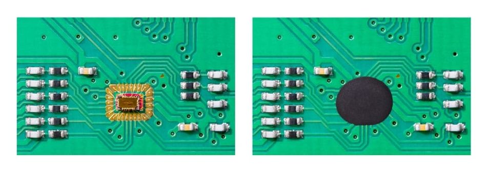
Flip-chip die attach is an advanced die attachment technique that has gained popularity due to its potential for high-density, high-performance, and small form factor applications. In flip-chip die attach, the die is flipped so that its active side, containing the integrated circuit, faces the substrate. This is achieved through a series of bumps, typically made of solder, that electrically and mechanically connect the die to the substrate. Commonly used die-attach solder always exhibits a thermal oxidation characteristic when it is in the liquid form. When the iron plating on the tip turns into iron oxide, which is a natural component of the metals used, solder tip oxidation is generated. At normal temperature, oxidation will take place, but considerably more slowly. Soldering heat significantly speeds up this procedure.
Flip-chip is comparable to wire bonding. Wire bonding does away with the necessity for high-heat assembly procedures, just like die attach. An adhesive or a eutectic alloy (a mixture of metals with the lowest feasible melting point) is used to adhere silicon chips (also known as "dice") to the package, substrate, or another die. After the dicing procedure, a chip is fixed to a substrate using die bonding, and electrical signals are secured using wire bonding, which is done after die bonding.
The bump formation process is a critical aspect of flip-chip die attach. Electroplating and stencil printing are two common methods for creating solder bumps. Electroplating, for instance, can produce bumps with diameters ranging from 25 µm to 150 µm, while stencil printing can create solder paste deposits as small as 50 µm in diameter.
One of the primary advantages of flip-chip die attach is the reduction in interconnect length. By flipping the die, the distance between the die and the substrate is minimized, which results in lower inductance, capacitance, and resistance. This translates into improved electrical performance, allowing for higher signal transmission speeds and reduced power consumption.
Thermal management is another key aspect of flip-chip die attach. Due to the direct contact between the die and the substrate, heat can be dissipated more effectively. For instance, attaching a high-power GaN die on a copper coin substrate using flip-chip technology can result in thermal resistance as low as 0.1°C/W, significantly improving the device's heat dissipation performance.
Flip-chip die attach also enables a higher level of integration. Since the active side of the die faces the substrate, additional components, such as passive devices or other integrated circuits, can be mounted on the same side of the substrate. This allows for greater component density and smaller overall form factors.
Underfill material is often used in flip-chip die attach to enhance the mechanical and thermal reliability of the assembly. By filling the gap between the die and the substrate, the underfill material helps distribute mechanical stress, reducing the risk of solder joint fatigue or cracking. Typical underfill materials exhibit a coefficient of thermal expansion (CTE) between 20 ppm/°C and 45 ppm/°C, which is compatible with both the die and the substrate.
In summary, flip-chip die attach offers several advantages, such as improved electrical performance, enhanced thermal management, and increased component density, making it a promising technique for advanced semiconductor applications. This aspect, as found in die-attach and thermal management is common with automotive electronics. Sometimes called power semiconductors, they are used in automotive ignition systems, and AC and DC electric motor drives of all sizes.[8]
Conclusion
In the semiconductor industry, die attach is a critical step in the fabrication of electronic devices. The process influences the device's performance, reliability, and lifespan. Advanced die attach techniques, such as laser die attach and flip-chip die attach, have been developed to meet the demands of modern high-performance, high-density applications. While each technique has its strengths and challenges, they all strive to achieve optimal thermal management, reliable mechanical adhesion, and efficient electrical interconnection. As the industry continues to push the boundaries of miniaturization and performance, new die attach techniques and materials will undoubtedly emerge, furthering the advancement of electronic devices.
Frequently Asked Questions (FAQs)
What is die attach? Die attach is the process of attaching a die, or chip, to a substrate or package in the fabrication of electronic devices. It serves to provide mechanical adhesion, electrical interconnection, and thermal management.
What is the purpose of die attach? The primary purposes of die attach are to provide a mechanical bond between the die and the substrate, establish electrical connections, and manage heat dissipation. The quality of die attach can significantly affect the device's performance and reliability.
What is a die attach material? A die attach material is the substance used to adhere the die to the substrate or package. Common die attach materials include epoxy-based adhesives, silver-filled glass frits, and various types of solder. The choice of material depends on the specific requirements of the device, such as operating temperature, power density, and reliability.
What are some advanced die attach techniques? Advanced die attach techniques include laser die attach and flip-chip die attach. Laser die attach uses a laser to melt the die attach material, enabling precise control of the process. Flip-chip die attach involves flipping the die so that its active side faces the substrate, reducing interconnect length and improving electrical performance.
What factors influence the choice of die attach technique and material? Several factors influence the choice of die attach technique and material, including the thermal and electrical requirements of the device, the mechanical stress the device will be subjected to, the operating environment, the intended lifespan of the device, and cost considerations.
Reference
Ghaffarzadeh, K., 2019. Die Attach Materials for Power Electronics in Electric Vehicles. Available at: https://www.idtechex.com/en/research-article/die-attach-materials-for-power-electronics-in-electric-vehicles/18438 [Accessed 23 May 2023]
Oricus Semicon, 2021. What is die attach process? Available at: https://oricus-semicon.com/what-is-the-die-attach-process/ [Accessed 23 May 2023]
Piaopiao He, Jinlong Zhang, Jianhua Zhang, Luqiao Yin, "Effects of Die-Attach Quality on the Mechanical and Thermal Properties of High-Power Light-Emitting Diodes Packaging", Advances in Materials Science and Engineering, vol. 2017, Article ID 8658164, 8 pages, 2017. https://doi.org/10.1155/2017/8658164
Thomas, M., n/a. Die attach materials and process. Available at: https://sst.semiconductor-digest.com/2007/04/die-attach-materials-and-processes/ [Accessed 23 May 2023]
Baghria, G.S, et al, [2012]. Die Bonding Techniques and Methods. Available at: https://www.eetimes.com/die-bonding-techniques-and-methods/ [Accessed 24 May 2023]
Inseto, 2020. Die Attach Process: Guidance & Setup. Available at: https://www.inseto.co.uk/setting-up-the-die-attach-process-ikb-072/ [Accessed 24 May 2023]
Kim S. Siow, 2019. Die-Attach Materials for High-Temperature Applications in Microelectronics Packaging. DOI https://doi.org/10.1007/978-3-319-99256-3
Gisler, W. and Connel, K., n/a. Die Attach. Available at: https://sst.semiconductor-digest.com/2000/03/die-attach/#:~:text=In%20simple%20terms%2C%20die%20attach,80%20percent%20of%20manufacturers%20today. [Accessed 25 May, 2023]
in this article
1. Introduction2. Fundamentals of Die Attach3. Importance of Die Attach4. Materials Used in Die Attach5. Die Attach Methods6. Process Parameters in Die Attach7. Die Attach Quality and Reliability8. Advanced Die Attach Techniques9. Conclusion10. Frequently Asked Questions (FAQs)11. Reference