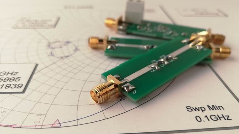
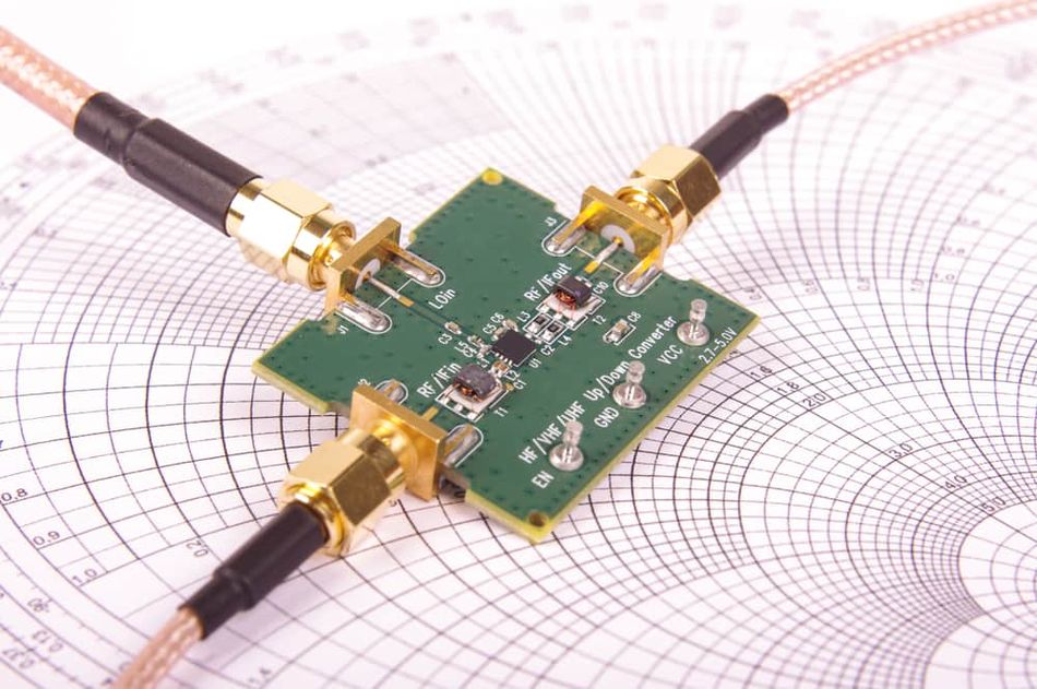
Controlled Impedance: A Comprehensive Guide
Controlled impedance in printed circuit boards involves the regulation of resistance exerted by signal traces. It is determined by characteristic factors of PCB fabrication, such as trace width and copper thickness. This article discusses controlled impedance and the essentials of its execution in PCB manufacturing.

26 Jan, 2023. 12 minutes read
PCB Impedance Calculation
No time now? Save for later.
We only use your email to send this link. Privacy Policy.
Introduction
Controlled impedance is the regulating impedance levels in PCB signal traces. It involves the process of measuring the impedance of certain traces in a PCB when it is being manufactured and making sure that they adhere to the limits stipulated by the designer.
Despite being costly, this method gained popularity around the turn of the century as a result of the steadily rising frequencies of electrical components. It is used in many different applications, including analog and digital telecommunications, video signal processing, web boxes, TV, GPS, video games, digital cameras, computers, tablets, mobile phones, and motor control modules, among others.
Reactance and resistance combine to create impedance in printed circuit boards. It is used to gauge the resistance of a current against an applied alternating current. Impedance as a property of AC is related to the frequency and is usually measured in ohms (Ω).
Whenever a signal travels through a conductor with the same impedance as another specified impedance, the transmission is perfect. But signals may be impacted if the impedance is varied on both sides. Controlled impedance is typically applied in single-ended microstrip, embedded microstrip, stripline differential pair, and planar PCB transmission lines.
When the trace impedance is well-controlled, it indicates that it is constant along the whole PCB path. This implies that the impedance should be constant throughout the component, from the source to the destination, regardless of where the trace travels or whether it changes layers. Although not much can be done about the impedance in the driver or the load, it can be adequately managed on the PCB. Therefore, it is preferred to have circuitry on the PCB that is properly matched to the source and load's impedance. As a result, there is an assurance of a consistent appearance along the entire path of the PCB.
To achieve this impedance, there are a few essential design criteria that must be taken into consideration. It is pertinent to note that many of the problems relating to reflections with regard to EMI can be averted by good PCB design techniques.
What is Controlled Impedance in PCB?
Controlled impedance involves controlling the resistance that a signal trace exerts on a signal. PCB traces are meant to generate signal power and transfer it from the driver device to the receiving device. ie, they carry electric signals between connecting parts. This signal power is expected to spread through the length of the trace.
Recommended reading: Trace PCB: A Comprehensive Guide
However, the signal movement can be impacted, as it takes time for them to travel along the transmission lines. Depending on several different factors, such as materials, the time delay can increase or decrease.
Therefore, controlled impedance is the matching of substrate material properties with trace dimensions and locations to ensure the impedance of a trace's signal meets a specific value or range. Controlled impedance ensures smooth signal transmission from source to destination.
What are the Three Types of Controlled Impedance?
Three common divisions of characteristic impedance controls are single-ended, differential, and coplanar impedance control.
Single-Ended Impedance
Single-ended impedance control is the impedance on a certain length of a trace or a single signal line. This requires calculation to determine the level of trace modification, as well as material matching and board stack-up adjustments. After this, the impedance-controlled PCB fabrication commences. This type of impedance control can be measured on a single trace, usually not coupled to the adjacent line.
The single-ended impedance is affected by PCB substrate height, substrate dielectric Er value, the lower and upper trace width, trace copper weight, and coating. However, the main determining factors here are dielectric Er value and trace width.
Differential Impedance
Another commonly used impedance type in printed circuit board design and manufacturing is differential impedance. This is the impedance between two transmission lines, also known as differential pair traces, of equal width and equal spacing during the differential drive.
The differential impedance is affected by PCB substrate height, dielectric Er value, trace widths, trace spacing, trace copper thickness, and coating. The major factors to consider during calculation, however, are substrate height, Er value, trace width, and spacing.
Coplanar Impedance
Coplanar impedance control refers to the impedance measured when the signal line is transmitted between GND/VCC around it.
This impedance type has a grounded coplanar waveguide structure, where there is a coplanar ground plane a controlled distance away from the trace that is close enough to considerably affect the impedance of the trace.
Why is Impedance Control Required?
Impedance control is essential to maintain signal integrity for high-frequency usage. High-frequency applications like digital and analog telecommunications, computers, phones, tablets, etc have highly complex designs. They require controlled impedance to protect data from damage and to provide a clear signal to all devices. The significance of controlled impedance is further outlined below:
Regulates the flow of electricity in the printed circuit board.
Controls and regulates the electrical flow as the device requires.
Stabilizes the signal integrity in complex designs and high frequencies.
Important for maximum signal integrity in printed circuit boards.
Calculating uncontrolled impedance is challenging when the components are mounted on a PCB. This is because components' tolerances vary based on their materials, etc. Additionally, temperature changes have an impact on component specifications, which leads to product malfunction. Swapping out a component may seem like the best course of action in this case, but the problem is often caused by a single inappropriate trace.
It is therefore crucial to gauge each trace's impedance before the PCB design is complete. Making a PCB compliant with the necessary values requires close collaboration between designers and manufacturers.
What Factors Affect Controlled Impedance?
Several factors can affect impedance control. They include trace width, copper thickness, dielectric thickness, and dielectric constant.
Trace Width: This is the width of the copper foil on a PCB, as well as its coating. Increased trace width leads to decreased impedance. In PCB design, trace width is specified based on a few different factors, and it is at this stage that the required impedance is accounted for.
Copper Thickness: This is another factor that affects impedance on a PCB. Like trace width, a rise in copper thickness leads to a fall in impedance.
Dielectric Thickness: This refers to the thickness of the insulating material between traces. A high increase in thickness usually results in modest increases in impedance, due to the logarithmic relationship between them. Reducing impedance through this requires a substantial reduction of the thickness of the insulating material.
Dielectric Constant: This is the ratio of the electric permittivity of a material to the electric permittivity found in a vacuum. A PCB with a low, stable dielectric constant is appropriate for high frequencies and controlled impedance. [1]
Why is it Good to Specify the Dielectric of the Board Instead of CI?
The impedance of traces is largely dependent on the materials used on the printed circuit board. The dielectric constant of the materials and the projected impedance conditioned by some specific parameters is called a controlled dielectric. Using the controlled dielectric approach to control the impedance requires complex calculations. Once this is done, the exact required dielectric space between copper layers can be specified in the design, to properly direct the trace layout during fabrication. [2]
How to Design a Board With Controlled Impedance?
Designing a circuit board with controlled impedance requires the application of the following strategies:
Determine which signals require CI
Electrical engineers usually specify the controlled impedance signals' values and types so that the layout team understands which nets are single-ended or differential pairs. Datasheets usually provide detailed guidelines for each group of signals and their impedance values. The spacing regulations and data on which later to route specific signals may also appear in the datasheets.
Annotate the schematic with impedance requirements
The design engineer draws up the circuit schematics, as one of the initial stages of board design. During this process, he specifies controlled impedance signals in the schematic and classifies specific nets to be either differential pairs or single-ended nets. The engineer may also specify precise layout design guidelines for controlled impedance to be followed by the layout designer, either in the schematic or in a separate “Read Me” file.
Determine the trace parameters for controlled impedance
A PCB trace is characterized by its thickness, height, width, and dielectric constant of the PCB material where the traces are etched. Designing controlled impedance PCBs requires careful consideration of these parameters. The number of layers, the value of the impedance traces on specific layers, and the materials for PCB fabrication can be specified for the manufacturer.
Apart from producing a stack-up that details the number of layers, trace width on each layer, the thickness of each dielectric, trace thickness, and board material, the manufacturer satisfies the impedance control requirements by calculating the practicable thickness, height, and width for the traces that require controlled impedance.
The following factors must be taken into account when routing to guarantee that the same impedance values are maintained along the whole controlled trace:
Trace geometry: This is the width and thickness of the trace being routed.
Signal spacing: The adjacent reference plane layer is typically where the distance between the signal trace and its return path is located. The configuration of the board layer stack-up will control this.
Dielectric material: This is the prepreg and core materials utilized on each side of the controlled impedance trace layer. The impedance calculations will take into account their thickness and dielectric constant.
To calculate the proper trace width for routing, PCB layout designers must add these parameters to the circuit's impedance specifications. The trace impedance calculators that design tools often provide can be used to do these calculations. In addition to several internet calculators and charts, there are circuit simulators that can perform these calculations. [3]
Avoid These Routing Mistakes When Designing for Controlled Impedance
Discussed in the following outlines are some routing mistakes to avoid when designing the PCB for controlled impedance.
Differentiate CI traces from other traces
It is necessary to be able to tell the controlled impedance trace widths apart from the other traces on the board. It enables the PCB manufacturer to rapidly locate them and, if necessary, adjust the trace width to achieve a particular impedance. It will be impossible for the PCB manufacturer to identify which signals are the regulated impedance traces, for instance, if you need a 5mil trace to achieve 50 ohms impedance, having routed other signals with a 5mil width. For this reason, the 50 ohms impedance traces should be 5.1 or 4.9 mils wide.
Maintain symmetry in differential pair routing
Signal traces of high-speed differential pairs must be routed parallel to one another with a fixed distance between them. Calculating the specific differential impedance requires knowledge of the trace width and spacing. It is necessary to route the differential pairs symmetrically. Also, reduce the amount of space where pads or ends cause the specified gap to expand.
Placement of components, vias, and coupling capacitors
Components or vias should not be placed between differential pairs, even if the signals are routed symmetrically around them. Components and vias create a discontinuity in impedance and could lead to signal integrity problems. For high-speed signals, the spacing between one differential pair and an adjacent differential pair should not be less than five times the width of the trace (5W). You should also maintain a keep-out of 30mils to any other signals. For clocks or periodic signals, you should increase the keep-out to 50mils to ensure proper isolation.
Even if the signals are routed symmetrically around differential pairs, components or vias shouldn't be installed in between them. Signal integrity issues may result from the discontinuity in impedance caused by components and vias. The distance between one differential pair and an adjacent differential pair for high-speed signals shouldn't be less than five times the trace's width (5W). Additionally, a 30mil distance from any other signals should be maintained. To achieve proper seclusion for clocks or periodic signals, the distance value should be upped to 50 mils.
Length matching
When several high-speed signals are expected to arrive at their destination concurrently, length matching may be necessary (within a specified mismatch tolerance). If the signal speed on different traces is the same, length matching will approximate propagation delay.
The lengths of the traces that make up a differential pair must be very tightly matched; otherwise, the positive and negative signals would be mismatched. The use of serpentines in the shorter trace is required to make up for the length discrepancy. To lessen impedance discontinuity, the geometry of serpentine traces must be properly selected.
The serpentine traces should be placed very close to the source of the mismatch. This ensures the quick correction of the mismatch.
Bends also create mismatching, which reduces the size of the inner bend's trace relative to the outer bend's trace. As a result, serpentines should be placed as close as possible to the bend. If two bends in a pair are closer together than 15mm, they balance one another out. Due to this, the serpentines can be left out.
Each segment of a differential pair signal that bends as it moves from one layer to another utilizing vias must be matched separately. s Serpentines should be positioned on the shorter traces close to the bend. Since the lengths of the total signals will be closely matched, DFM checks will not find this infraction, thus a manual check should be performed. It is advised to route differential pair signals on the same layer if they need length matching because the signal speed of traces on separate layers may vary.
Reference layers for the return path of controlled impedance signals
A constant reference plane is necessary for the return path of all high-speed transmissions. One of the most frequent causes of EMI and noise coupling is an improper signal return path. While the return current for low-speed signals takes the shortest route possible, the return current for high-speed signals closely follows the signal path. High-speed signal return paths are typically provided in the reference planes closest to the signal layer.
Since the return path will not be able to follow the trace, high-speed communications should not be transmitted over a split plane. The trace should be routed around the split plane, to ensure greater signal integrity. It is also pertinent that the ground plane be at least three times the trace width on each side. This is known as the 3W rule.
A stitching capacitor must be placed between the two reference planes if a signal is to be routed over two distinct reference planes. To keep the distance between the signal and the return path as short as possible, the capacitor must be linked to the two reference planes and positioned near the signal path. The capacitor reduces impedance discontinuity and permits return current to flow from one reference plane to the other. The range of 10nF and 100nF is a suitable value for the stitching capacitor.
Slots in the reference plane immediately below the signal trace and blocks in the split plane should as well be avoided. To lessen the problems brought on by the divided return path, stitching vias should be utilized if the slots cannot be avoided. Moreover, the two pins of the capacitor should be placed close to the signal and connected to the ground layer.
Vias that are placed together tend to produce voids in reference planes. Staggering the vias to enable adequate feed of the plane between vias would reduce these huge voids. This via staggering also ensures that the signal has a continuous return path.
Ground planes are usually preferred as a reference. However, if a power plane is used as a reference plane, a stitching capacitor should be introduced to allow the signal to change the reference from the ground to the power plane and then back to the ground.
A capacitor with one end connected to the ground and the other to the power net should be placed close to the signal input and exit locations.
Add stitching vias close to the layer change vias.
Stitching vias should be added near the layer change vias if a high-speed differential pair or single-ended signal shifts layers. Doing this will also allow the return current to switch ground planes.
Recommended reading: What is a Via: A Comprehensive Guide
If a high-speed signal trace switches to a layer that has a different net as reference, stitching capacitors are needed to enable the return current to pass from the ground plane through the stitching capacitor to the power plane. For differential pairs, the capacitor arrangement needs to be symmetrical. [4]
Key Takeaways
Impedance control is the process of regulating the strength of a PCB's traces by measuring its impedance. Impedance control has become a PCB standard practice due to the constantly changing frequencies of new devices and high-tech applications.
After the PCB is fabricated, impedance control can be confirmed using test coupons. A test coupon is a PCB used to gauge the effectiveness of a PCB production process. Test coupons are made on the same panel as the PCBs, usually around the edges. After that, coupons are examined to check for appropriate layer alignment, electrical connectivity, and internal structure. Coupons may be chosen from a vendor collection or created specifically for a PCB. The PCB manufacturer can be tasked to design a test coupon or they can place test coupons on functional panels.
A decent cross-section of the PCB will be represented by the placement of test coupons on the working panel, which are usually distributed among several locations. The impedance can then be measured using a Time-Domain Reflectometer (TDR). A report will then be produced to show whether the characteristic impedance was attained on the PCB.
References
1. My EMS Solutions. Impedance Control in PCB: Everything You Need to Know. 2021. [Cited 2023 Jan 22] Available from: https://www.myemssolutions.com/impedance-control-in-pcb-everything-you-need-to-know/
2. Sierra Circuits. PCB Substrates: Knowing Your Dielectric Material's Properties. 2022. [Cited 2023 Jan 22] Available from: https://www.protoexpress.com/blog/pcb-substrates-knowing-dielectric-materials-properties/
3. RayMing. Why is PCB Impedance Control so Important. 2021. [Cited 2023 Jan 23]
4. PCB HERO. How to Avoid These Routing Mistakes When Designing for PCB Impedance. 2022. [Cited 2023 Jan 23] Available from: https://www.pcb-hero.com/blogs/lilycolumn/how-to-avoid-these-routing-mistakes-when-designing-for-controlled-impedance
in this article
1. Introduction2. What is Controlled Impedance in PCB? 3. What are the Three Types of Controlled Impedance?4. Why is Impedance Control Required?5. What Factors Affect Controlled Impedance?6. Why is it Good to Specify the Dielectric of the Board Instead of CI?7. How to Design a Board With Controlled Impedance?8. Avoid These Routing Mistakes When Designing for Controlled Impedance9. Key Takeaways 10. ReferencesNo time now? Save for later.
We only use your email to send this link. Privacy Policy.