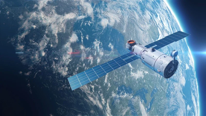
The Role of JFETs in Satellite Systems: Enhancing Signal Amplification in Radiation Environments
JFETs are vital components in satellite systems due to their low-noise performance, high input impedance, and superior radiation tolerance.

30 Apr, 2025. 6 minutes read
Reliable signal amplification is an absolute necessity in all satellite systems. Whether facilitating deep-space communication, managing telemetry and control, or processing signals from scientific instruments, satellites depend on stable, low-noise amplification to guarantee data integrity. Yet, the harsh conditions of space present formidable challenges for conventional semiconductor devices, often resulting in performance degradation or outright failure over time.
Here, Junction Field-Effect Transistors (JFETs) are a saving grace. As depletion-mode devices with inherently high input impedance and minimal gate leakage current, JFETs preserve signal fidelity even in the reaches of space. This paper explores the structural advantages, radiation tolerance, and application-specific benefits that make JFETs the go-to solution for spaceborne signal amplification.
Understanding JFETs: Structure and Operational Principles
JFETs are depletion-mode devices that regulate current through a reverse-biased PN junction. To this end, each JFET consists of three terminals: source, drain, and gate. The core of the device is a doped semiconductor channel (i.e., typically n-type for N-channel JFETs) through which current flows from source to drain. The gate, formed by heavily doped p-type material, is placed adjacent to the channel and remains reverse-biased. By adjusting the gate-to-source voltage (VGS), the depletion region expands or contracts, narrowing the conductive channel and modulating current flow.

Compared to MOSFETs, which can operate in both depletion and enhancement modes, JFETs operate solely in depletion mode. Critically, the absence of a gate oxide layer makes JFETs more resilient to total ionizing dose effects, granting them superior tolerance to radiation-induced degradation in space environments.
An additional defining characteristic of JFETs is their extremely high input impedance, typically ranging from 10^9 to 10^12 ohms. This impedance characteristic minimizes the loading effect on preceding circuitry, which is necessary for maintaining signal integrity in weak analog systems. Additionally, their unipolar conduction and lack of minority carrier injection make JFETs exhibit inherently low noise in signal amplification applications. Meanwhile, their low power consumption is a perfect match for the tight energy requirements of satellite platforms.
Challenges of Space Radiation and Its Impact on Semiconductor Devices
The space environment exposes electronic systems to persistent and intense radiation that significantly affects the performance and reliability of semiconductor devices. Generally, the two principal types of radiation effects are Total Ionizing Dose (TID) and Single Event Effects (SEE).
Total Ionizing Dose refers to the cumulative damage caused by prolonged exposure to ionizing radiation, such as electrons and protons trapped in Earth's magnetosphere or emitted from the sun. Over time, these charged particles deposit energy into device materials, such as the gate oxide of MOS-based devices. This results in the buildup of trapped charge, which shifts threshold voltages, increases subthreshold leakage currents, and leads to device parameter drift or functional failure.
Single Event Effects are induced by high-energy particles, such as heavy ions or cosmic rays, that strike a device and generate transient currents or localized disruptions. These can manifest as soft errors like single event upsets (SEUs) or more damaging phenomena like single event latch-up (SEL), which may lead to catastrophic failure if not mitigated.
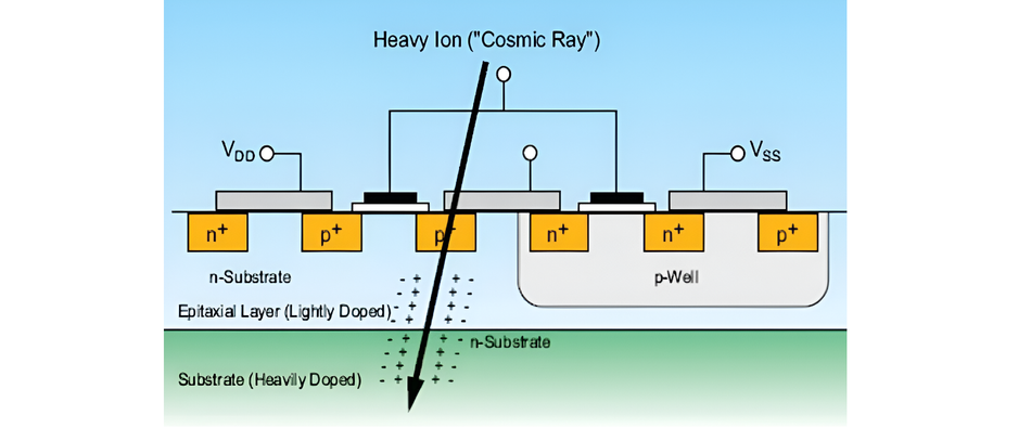
Traditional semiconductor technologies are particularly vulnerable in these conditions. MOSFETs, for instance, suffer from radiation-induced charge trapping in their gate oxide, resulting in threshold instability and increased leakage. Bipolar Junction Transistors (BJTs) face degradation in current gain due to increased recombination rates from radiation-induced defects in the base region. These skewed characteristics ultimately compromise their amplification capabilities over time.
In contrast, JFETs demonstrate superior resilience to both TID and SEE. Structurally, JFETs lack a gate oxide layer, thereby eliminating the primary site for charge trapping. This structural simplicity means that gate threshold stability is maintained even under significant radiation exposure. Furthermore, JFETs inherently operate with low leakage current, allowing them to remain largely stable under radiation and preserve the signal integrity required in sensitive analog circuits.
Importantly, JFETs are less susceptible to latch-up events than their competitors. SEL typically arises from parasitic thyristor action in CMOS devices that is triggered by ionizing particle strikes. JFETs, however, do not possess the requisite structures for this mechanism, making them naturally robust against latch-up. Their radiation hardness, low noise operation, and stable electrical behavior make JFETs particularly well-suited for amplifying small signals in radiation-intensive environments.
Advantages of JFETs in Satellite Signal Amplification
JFETs offer a suite of electrical and physical properties that align exceptionally well with the demanding requirements of satellite signal amplification.
Low Noise Performance
One of the most valuable attributes of JFETs is their exceptionally low-noise performance, particularly in the 1/f (flicker) noise region. In satellite systems, signals from distant sources can be extraordinarily weak and easily overwhelmed by internal circuit noise. Low noise JFETs are therefore necessary to effectively detect and amplify extremely weak signals. Their minimal noise contribution allows for clearer signal acquisition without the need for excessive post-processing or error correction for simpler and more reliable systems.
High Input Impedance
The input impedance of a JFET is typically on the order of 10^9 to 10^12 ohms. This characteristic is especially beneficial in satellite payloads that incorporate high-impedance sensors such as photodiodes, electrometers, or piezoelectric transducers. A JFET's minimal gate current ensures that it does not load the signal source, thus preserving amplitude and spectral fidelity throughout the signal chain.
Stability Across Temperature
JFETs’ remarkable stability across extreme temperature ranges is a crucial feature given that spacecraft components must operate under thermal fluctuations spanning from -200°C to +150°C. Where bipolar or CMOS transistors experience significant parameter drift under such conditions, JFETs maintain consistent transconductance and threshold characteristics regardless of temperature. Therefore, JFETs can help ensure predictable circuit behavior across orbital day-night cycles and interplanetary mission phases.
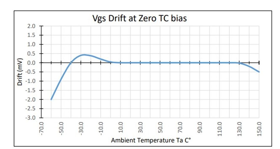 JFET VGS drift versus temperature. (Source: InterFET)Power Efficiency
Satellites are expected to operate indefinitely without being serviceable for battery changes or charging. That means power consumption is important.
JFETs consume significantly less power than their bipolar counterparts on account of their gate being reverse-biased and drawing virtually no steady-state current. Their low quiescent current requirements and passive gate operation minimize overall power consumption without compromising performance.
Radiation Tolerance
Finally, JFETs display strong resistance to radiation-induced parametric shifts. Prolonged exposure to space radiation tends to alter the behavior of most semiconductors, but JFETs show minimal variation in parameters like transconductance and pinch-off voltage. This intrinsic resilience simplifies radiation-hardening strategies and reduces the need for extensive shielding or redundant circuit paths.
Applications of JFETs in Satellite Systems
The unique electrical and environmental resilience of JFETs has made them ubiquitous across a wide range of satellite subsystems.
Communication Systems
In communication systems, JFETs are frequently employed in RF front-end amplification stages. Positioned at the input of receiver chains, they amplify incoming signals before downconversion to preserve signal-to-noise ratio (SNR) during the earliest and most important stage of processing. Their low noise figure and high linearity make them particularly effective in telemetry, tracking, and command (TT&C) applications, as the integrity of bidirectional communications between satellites and ground stations must be maintained over vast distances and through variable atmospheric conditions.
Scientific and Earth Observation
Scientific and Earth observation satellites rely heavily on JFETs for interfacing with sensitive instruments. These include circuits that require minimal noise and stable gain, such as those used for detecting cosmic background radiation, solar wind, and magnetic fields. JFETs are routinely used in analog front ends for magnetometers, radiation detectors, and spectrometers to enable accurate signal transduction from low-level outputs without introducing thermal or shot noise that could distort measurement precision.
Optical Systems
In space-based optical systems, JFETs are integral to the readout electronics of charge-coupled devices (CCDs) and infrared detectors. Their low input capacitance and noise allow for the clean extraction of pixel-level charge signals that unlock high dynamic range and sensitivity in space telescopes, astronomical observatories, and optical payloads tasked with deep-space imaging or Earth observation.
Power Management and Control
Lastly, JFETs support power management and control circuits in satellite subsystems. Their predictable saturation behavior and low gate current allow for linear regulation stages, reference voltage circuits, and current sources that are stable, efficient, and low-noise.
Conclusion
In the unforgiving environment of space, JFETs offer a uniquely robust solution for signal amplification. But, while the inherent properties of JFETs make them well-suited for space, achieving optimal performance requires careful circuit design. Factors such as biasing stability, thermal management, and layout strategies all impact gain and noise margins over time. As satellite missions push further into deep space and demand more precision from onboard instruments, these design considerations become increasingly important. Fortunately, JFETs, with their proven track record and evolving fabrication technologies, will continue to be integral to the future of satellite communication and scientific exploration platforms.
References
Siliconix AN101 – An Introduction to FETs
InterFET AN-015 – JFET Fundamentals
MOSFETs vs JFETs: Understanding Structures, Differences & Applications
CTC-028 JFET Radiation Resistance
Application Note: Discrete JFET versus JFET OP-Amp