ROHM's Advanced Packaging for Highly Efficient Power Electronics Systems
Rising power demands from emerging industries are pushing manufacturers to maximize the performance and efficiency of their power supplies. Using advanced power semiconductor packaging technologies is becoming essential to meet the next-gen targets.

19 May, 2026. 5 minutes read
Attention toward power supply design is higher today than ever before. This is because applications consuming large amounts of electricity, such as electric vehicles (EVs) and artificial intelligence (AI) servers, have emerged and are rapidly expanding their market size. As the global electricity demand rises, it is anticipated that power shortages will occur globally in the near future.
Building new power plants could avert this situation. However, power plants cannot be constructed overnight. Building a single new plant likely requires 5 to 10 years and significant capital investment. This timeline makes it difficult to address the rapidly increasing power demand driven by the extremely fast adoption rates of EVs and AI servers.
This is why efficient power usage is gaining attention. Increasing conversion efficiency from 96% to 98% may seem like a small improvement of just 2 percentage points; however, when dealing with large amounts of power, the reduction in power loss becomes significant. For example, for a 100 kW output power supply circuit, improving conversion efficiency by 2 percentage points would theoretically reduce power loss by approximately 2 kW.
Therefore, power semiconductor manufacturers are focusing their efforts on improving the performance of power semiconductor chips.
Reducing on-resistance cuts conduction losses, while improving switching characteristics (such as faster and more efficient switching transitions) reduces switching losses. There are many other ways, like improving the "packages" that encapsulate the power semiconductor chips. In addition to improving power efficiency, newer packaging technologies can improve thermal characteristics, potentially reducing the power consumed for cooling.
Why Packaging Matters in Power Semiconductor Devices
A package’s functions can be broadly categorized into four main areas:
Improving heat dissipation
Ensuring current capacity
Ensuring mechanical/environmental reliability
Improving mountability/mass-producibility
Packages that fulfill these basic roles can be broadly classified into three main types.
Through-Hole Package
Through-holes are created in the printed circuit board (PCB) for mounting. Representative shapes include TO-220, TO-247, and TO-264.
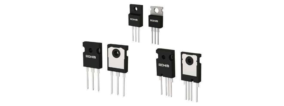
Advantages include ease of handling high currents and high voltage ratings due to the large size of the package and ease of mounting on heat sinks. Disadvantages include a large mounting footprint and unsuitability for automated mounting.
Surface-Mount Package
A surface-mount package is mounted by reflow soldering onto electrodes formed on the surface of the PCB. Representative shapes include DPAK (TO-252), D2PAK (TO-263), Power SO-8, LFPAK, DFN, and TOLL (TO-Leadless).
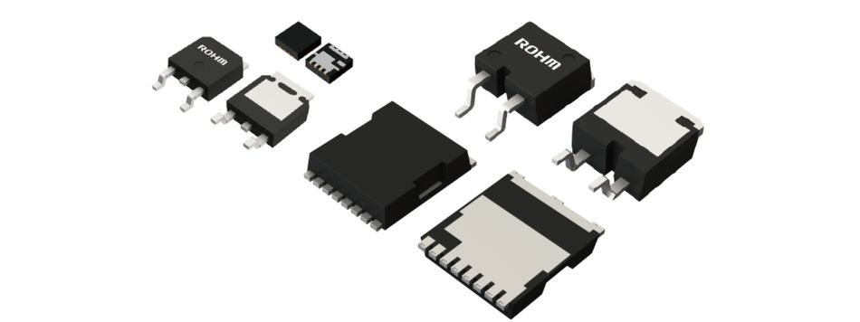
The advantages include enabling automated placement and high-density mounting, as well as allowing heat dissipation from the package's back side through thermal vias into the PCB interior. Disadvantages include limited thermal performance and the tendency for increased mounting density to affect surrounding electronic components due to heat generation. Top-side cooling (TSC) components can address these challenges with thermal management by dissipating heat. ROHM is advancing the development of a lineup that includes this type of packaging, such as Q-DPAK, TSC3, and TOLT.
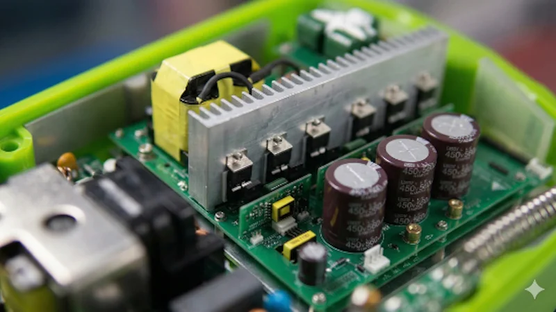
Power Module
Power modules differ significantly from through-hole and surface-mount packages. While through-hole and surface-mount packages essentially encapsulate a single power transistor chip, a power module houses multiple power transistor chips, diodes, and other components. Examples include a 6-in-1 module with six power transistor chips for three-phase inverters or a 2-in-1 module with two power transistor chips for half-bridge circuits.
Advantages include simplified design of power circuits like inverters, enabling high-density mounting, high compatibility with cooling methods such as baseplates or liquid cooling, and easier mitigation of radiated noise (EMI). A disadvantage is the higher cost compared to using devices packaged in through-hole or surface-mount types.
Improvement in Packaging
There are three points of improvement in these packages. Specifically, they are:
Improvement of electrical characteristics
Improvement of thermal characteristics
Standardization
Improvements in Electrical Characteristics
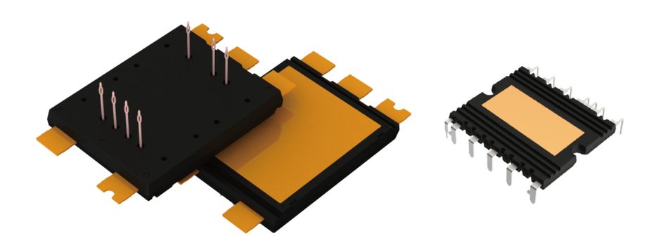
A typical method for improving electrical characteristics is to switch to wire bonding-less technology. Normally, the lead frame (the metal part that holds the chip) and the chip are connected by a thin metal wire. However, thin metal wires tend to have high parasitic inductance and parasitic resistance. Wire bonding-less technology replaces the thin metal wire with a copper clip that has a larger surface area. Connecting with a copper clip widens and shortens the current path, both parasitic resistance and inductance.
The Kelvin source connection is another method for improving electrical characteristics. This technique splits the source terminal into two paths: one for high-current flow and another for voltage application. While not a new technology, it has regained attention with the proliferation of extremely high-speed SiC power MOSFETs and GaN HEMTs. This is because the Kelvin source connection enables stable gate drive even at high switching speeds. Consequently, it allows the full benefits of SiC power MOSFETs and GaN HEMTs to be realized, reducing switching losses in power supply circuits. Typically, power transistors have only one source terminal.

In a Kelvin source connection, the source terminal is divided into two paths, one for the high-current return and the other for voltage sensing, which reduces voltage bounce and enables stable gate drive operation.
Suggested reading: SCT4045DR - Data Sheet, Product Detail | ROHM.com
Furthermore, in power modules, the trend of integrating gate drive chips alongside multiple power transistor chips is accelerating. Particularly in power modules employing GaN HEMTs with extremely high switching speeds, integrating the mainstream gate driver chip is becoming more common. The extremely high switching speed makes gate drive circuit design very difficult. To address this issue, power semiconductor manufacturers are providing power modules that integrate gate driver chips specifically optimized for GaN HEMTs. This allows users to maximize the high performance of GaN HEMTs while ensuring the same ease of use as conventional Si power devices.
Suggested reading: Next-Generation GaN Power Device Development
Improvements in Thermal Characteristics
A representative technique for improving thermal characteristics is likely dual-surface heat dissipation. This involves building a package with heat dissipation electrodes on both the top and bottom surfaces. A heat sink contacts the top heat dissipation electrode to dissipate heat. Meanwhile, the rear heat dissipation electrode contacts a large-area electrode on the PCB surface, dissipating heat through the board's internal ground plane or similar paths. This approach lowers the package's thermal resistance, enhancing heat dissipation characteristics.
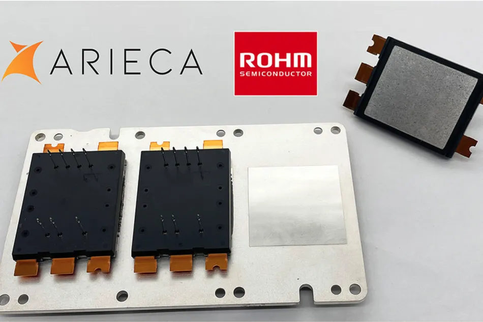
New materials to enhance thermal characteristics are also being developed for modules. For example, ROHM is collaborating with the US startup Arieca to develop Liquid Metal Embedded Elastomer (LMEE). This is a thermal interface material inserted between a module containing multiple power transistors and a heat sink, enabling improved thermal performance.
Standardization
Currently, power semiconductor (power transistor) manufacturers adopt their own unique packages, differing in dimensions and pin configurations. Consequently, power supply manufacturers, as end users, face challenges in sourcing from different suppliers. The burden of evaluating electrical/thermal characteristics when adopting new packages is also significant. Users have repeatedly raised these very concerns.
To address this issue and improve convenience for power supply manufacturers, a partnership has been established between Infineon Technologies and ROHM to mutually adopt and develop each other’s packages. The packages targeted for standardization include DOT-247, TOLT, DPAK, QDPAK, QDPAK Dual, and HDPAK. All support heat dissipation from the package surface (top-side cooling) and have a package height of 2.3 mm. Target applications include onboard chargers, solar power inverters, energy storage systems, and AI data centers.
High-Efficiency Power with Advanced Packaging
As power density increases in semiconductor devices, packaging becomes a critical driver of performance. Semiconductor manufacturers continue expanding their portfolios and enhancing product performance to support higher-efficiency power systems.