Putting high-performance computing into cars: automotive discrete semiconductors for autonomous driving
Reliable, small, and lightweight hardware that meets increasing performance requirements is today’s engineering challenge in the automotive industry.
Last updated on 05 Aug, 2020. 11 minutes read

Automotive semiconductors are getting smaller and lighter. Image: Nexperia
This article is part of a series about ADAS and Autonomous Vehicles, sponsored by Nexperia. The first article provided an introduction on ‘How Advanced Driver-Assistance Systems (ADAS) Impact Automotive Semiconductors.’
In this second article, we will dive deeper into how new semiconductor products can increase reliability and performance as the demands of electrical automotive systems increase.
Autonomous driving requires tremendous computational resources. The current trend of high-level ADAS architectures is a central design; uncompressed video, LiDAR, and other sensor data is sent directly to central computing units.
Depending on the resolution and sensor types, high-speed interfaces are used to send the data from the sensor devices, such as cameras, to the central processing unit (often called ADAS box or ADAS processing unit). Looking at today’s reference designs presented by various automotive Tier1s, these boxes need to able to process several Gb of data per second. As the number of cameras and sensors, like zonal LiDAR, is increasing, it is clear that the requirement of fast data processing is increasing as well. To design reliable hardware that is not too big or too heavy to fit into the car is today’s design challenge in the automotive industry.
Ordinary PC-like computing platforms are not powerful enough to satisfy the hunger for the ever-increasing demands of data processing. The flagship ADAS reference implementations rather look like mid-range server-like architectures: Very often with dedicated GPUs optimized for self-learning algorithms. From a hardware perspective, this means that within the computing unit multiple high-power microchips need to operate and communicate, consuming vast amounts of energy.
When comparing the overall system requirements to a static server, it becomes obvious that reliability and functional safety are much more important for ADAS applications. In self-driving cars, redundant systems are typically used for super safety functions like electronics braking or steering. Many electronic functions are just single-function circuits. To save human lives, the reliability of the hardware is crucial in self-driving cars.
Centralized versus Decentralized Architectures for ADAS
In recent years, the expert community discussed distributed versus centralized ADAS concepts. Despite conceptual pros and cons, the reality is that low-level ADAS implementations are often distributed, and high-level ADAS concepts are rather centralized. The fundamental reason is that algorithms can make better and more reasonable decisions when using the data of multiple sensors at the same time. The preprocessing of the data near the sensor potentially increases the latency and reduces the ability to identify and observe an object as well as predicting its behavior based on various sensor data simultaneously.
Hence, the architecture of high-level ADAS concepts is a star-shaped topology, with one or more high-speed computing units in the center and various sensor units placed around the car. This choice has two consequences:
- There are many high-speed communication links between sensors and the central unit to transmit raw data with low latency, and
- The computing power of the central unit has to be significant to process the data from various sensors simultaneously and make reasonable decisions.
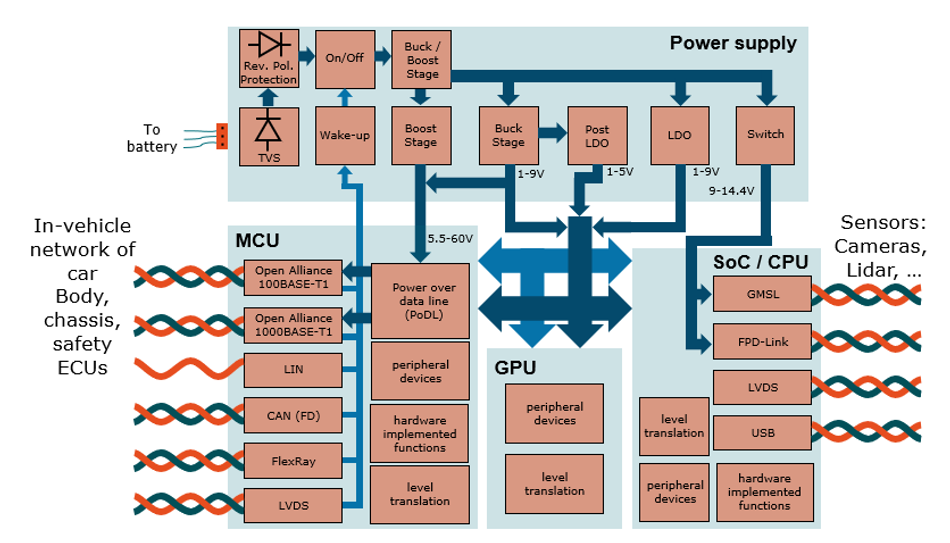
To understand what such a central processing unit looks like, we take a step back to the consumer industry: There is no fundamental difference between the principal architecture of a PC, a mid-range server, and a high-level ADAS processing unit. There has to be a power supply, there are CPUs and GPUs, microcontrollers for interfacing, as well as a bunch of microcontrollers that are managing the system by monitoring various parameters, loading firmware, turning on and off several parts of the system, and so on.
Recommended reading: How Advanced Driver-Assistance Systems (ADAS) Impact Automotive Semiconductors
These parts are crucial for the design and performance of a system and may, itself, be significantly different in PCs, servers, and ADAS applications. However, in none of these applications microcontrollers can function alone. To make them work, peripheral devices in the form of passive components, like resistors, inductors, capacitors, quartz, and discrete semiconductors in the form of Bipolar Transistors (BJTs), MOSFETs, standard logic like gates and buffers, ESD protection, as well as Zener, PN, and Schottky diodes are required.
Discretes and Integrated Circuits
Since the first integrated Integrated Circuits (ICs), experts proclaimed that discrete parts, especially logic, will all be integrated at one point in time and, therefore, will not be required in the near future. However, the reality looks different, even though an increasing amount of functionality has been integrated, discretes play an important role in system design because of four main arguments: flexibility, reliability, power, and cost.
Discretes bring flexibility because the huge portfolio of devices available allows designers to tune the application to their needs by selecting the right discrete, rather than redesigning the IC. Reliability comes from the fact that a discrete component only fulfills one functionality, so the production process and testing can be optimized.
Therefore, highly reliable single-function devices can be manufactured much more efficiently than a complex device. Especially for high current applications like power supplies, the ability to use a discrete to separate the power part from the IC is important.
To handle high currents, devices that act as switches or regulators must be large in order to keep the current density inside the device under a certain limiting value. From a system perspective, it is better to have a large switch or regulator as a dedicated discrete device optimized for this application and to keep the controlling IC separate.
Separation allows using a smaller and cheaper IC because they are not heated up by the current that is being controlled. This consideration does not only lead to increased system performance, but also to lower system costs, as a large IC is usually more expensive than a discrete component.
As the same discrete components are used in various applications, the very high volumes lead to much lower prices than ICs. Hence, discrete components are still a part of modern system design and play a crucial role in the toolbox of system designers.
Discrete components come in various shapes. Twenty years ago, engineers used “through-hole” packages, where the leads of the package penetrates the PCB. Especially in DIY projects and prototyping these are still in favor because of easy handling. For mass production, however, they are not state-of-the-art and are hard to find when tearing down a modern electronic product. The more modern version is called Surface Mount Device (SMD), where the device is soldered on the surface of a PCB.
SOT23
This technique allows for:
- Much denser packing of devices on a PCB with higher reliability, and
- For populating it on both sides, enabling modern electronic products.
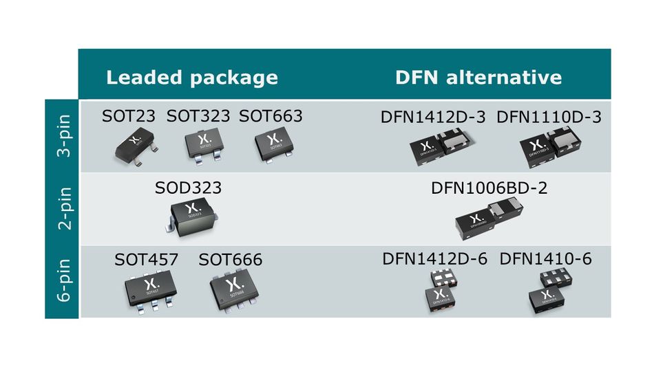
The most famous discrete SMD package is the SOT23, which was introduced by Phillips Semiconductors fifty years ago. Today, it is by far the most sold package.
The SOT23 family consists of; the original SOT23, which is a three-pin package often used for Bipolar Transistors (BJTs), small-signal MOSFETs, and (dual) diodes, the SOT457 (or TSOP6, SOT23-6), the six-pin version, used for dual BJTs and small-signal MOSFETs or logic devices, and the SOD323 which is the two-pin diode version.
The plastic is always the same size, and the leads are sticking out of the side of the package and are bent down to be soldered onto the PCB. The area on the PCB that is need for a footprint to solder a three- or six-pin package is roughly 4.6 mm times 4.5 mm in size. When looking at a smartphone, this size seems to be huge, but for PCs, TV sets, and automotive control units like engine control, body control, or infotainment, this package family is still the first choice.
However, central ADAS computing units and more sophisticated body control units increase the demand for a smaller alternative that provides the same reliability.
A new approach to discretes is required
Before looking at the technical details of miniaturized discretes for automotive applications, let’s have a look at how many discretes are actually required in a centralized ADAS computing unit.
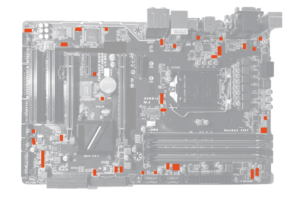
To get a rough understanding, let's again take a look at the PC. Figure 2 shows a motherboard of a standard PC. Highlighted, you see packages of the SOT23 family, housing various functionality.
On the motherboard there are 62 discrete devices in these standard packages; on a suitable graphics card, you find additional ca. 20 devices. Even though different CPUs, GPUs, and MCUs are being used in an ADAS box, it is reasonable to assume that a comparable amount of discretes is required to make the system work.
Modern ADAS computing platforms claim to use 1-2 CPUs and up to 4-8 GPUs. It follows that it’s reasonable to claim that “an ADAS computing unit consists of 50 to 250 discrete devices,” and it becomes clearer that a miniaturized alternative of the fifty-year of SOT23 family is required to for space-efficient system designs.
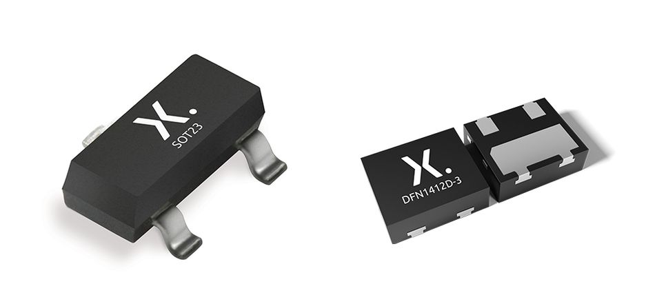
The novel alternative to the SOT23 family is called discrete flat no-lead, DFN. The principal chemical components of such a package are similar to SOT23s; the main difference comes from the geometry.
Figure 3 shows a 3D model of a SOT23 and a DFN1412D-3 to scale. This DFN package has about the same space inside the package as a SOT23 while being much smaller in total. The footprint required on the PCB to solder the DFN package is 80% smaller than the one required for SOT23. It can house the same silicon a SOT23 can, so the electrical parameters do not change, only the outline of the footprint gets smaller. When comparing both packages, it is evident that the space savings come from the removal of the leads.
For the SOT23 package, the leads stick outside the side of the plastic and are bent down to be soldered on the PCB. For the DFN package, the plastic underneath the metal that belongs to the lead inside the package is removed. This way, it can be directly soldered to the PCB without requiring the actual leads outside the plastic. By removing the unnecessary leads and excess plastic, a DFN package is derived.
Comparing the same device in SOT23 and DFN, the electrical parameters are nearly identical, and in addition, the DFN package offers improvements in less parasitic capacitance and inductance, which come from the removal of the leads. Regarding physical parameters, you can expect changes, like improved thermal behavior.
Inspection
As addressed before, reliability is essential for ADAS applications. One aspect is the solder joint connection between the PCB and the device. It is necessary to assure during production that a solder joint is sound both electrically and mechanically. This task is usually done by X-ray diagnostics or camera inspection (generally called automated optical inspection or AOI). X-ray is needed to inspect ball-grid arrays and other hidden solder connections. AOI is used to inspect leaded packages by optically evaluating the meniscus the solder paste forms at the side of the leads. Compared to X-ray, AOI is significantly cheaper and faster, and is therefore preferred.
To make the solder joint that is usually hidden underneath a DFN package inspectable, DFN packages have the option of a side-wettable flank, called SFW. Here, there is a tin-plated metal strip at the side of the package, as it can be seen in Figure 3. Due to this feature, an optically inspectable meniscus is formed at the side of the DFN package, allowing to use the cost-efficient AOI tooling already in place for SOT23.
The mechanical reliability of the solder joint between a DFN package and the PCB itself fulfills all automotive norms and is tested accordingly. However, some engineers are hesitant to go to DFN packages because of bad experiences.
Concerns
Firstly, leadless packages in automotive have been introduced for high-power MOSFETs used in motor control applications. As the first products were introduced, some designers raised concerns about the reliability of the solder connections, as the package expands when the device heats up and shear forces apply to the solder joints leading to micro cracks.
Hence, the first choice of a designer of automotive power application is the cupper clip-bonded LFPAK (Loss-Free PAcKage), which can be seen as a combination of the benefits of DFN package and external bent leads that can mitigate the mechanical stress. For power applications this makes perfect sense.
However, for peripheral discretes used in the surrounding of CPUs, GPUs, and microcontrollers and that are usually housed in SOT23, this argument does not apply: Powerful MOSFETs in motor control applications have to handle high currents and will inevitably heat up, and therefore a large effort has to be spent on thermal design. On the contrary, most devices in SOT23 run at rather low power and their self-heating is usually not a system critical effect.
Furthermore, the relative comes into account. While powerful MOSFETs have usual package sizes of 5mm by 6mm, 8mm by 8mm or are even larger, the DFN alternatives for SOT23 are 1.4mm by 1.2mm or even smaller. So, the force applied on the solder joint during elevated temperatures is significantly smaller, and thus, the solder joint reliability of the DFN alternatives for SOT23 is given. This enables the use of DFN package as a highly reliable alternative for SOT23 in critical applications like ADAS processing units.

Thermal Performance
On top of saving space on the board, there comes a second benefit when using DFN packages. Due to the internal structure, the thermal performance is much better.
Figure 4 shows a thermal simulation of a SOT23 and a DFN1412D-3, inside there is the same silicon. The simulations considers a dissipated power inside the silicon of 250mW. In the SOT23 package, the heat that is generated inside the silicon has to dissipate through the leads to PCB. The PCB and, to a very small degree, the leads radiate the heat to the surrounding environment, which is assumed to have an ambient temperature of 25°C. In the DFN package however, the heat is dissipated through the metal heatsink inside the package directly to the PCB. It is obvious that the thermal connection of the DFN package is significantly better that the one of SOT23.
In this simulation, it leads to a difference in temperature of the silicon of 25°C. This difference is significant and has two main implications. First, it allows to drive higher power in such a package. But, as already argued before, it is not the goal to optimize a high-power design, but rather have a look at ADAS processing units, where these peripheral devices are used at low power. The much more important fact here is that the device runs cooler in the ordinary operation. This is directly related to an extended lifetime of the device in the application, leading to an increased overall reliability.
Conclusion
High-level ADAS computing units have a high demand of peripheral discrete components that allow for the highest reliability and small packaging size to enable high integration. The fifty-year-old industry-standard SOT23 is available and widely used. However, the technology is large and occupies significant board space. State-of-the-art DFN technology allows housing the same electrical functionality in significantly reduced package size allowing to use of an 80% smaller footprint.
Additionally, to the space savings, the technology leads to reduced operating temperature resulting in an increased system reliability. DFN alternatives exist for the whole SOT23 family: The standard diode package SOD323 goes with the DFN1006BD-2, SOT23 with DFN1412D-3 or DFN1110D-3, and the six-pin version SOT457 (TSOP-6) with DFN1412D-6 or DFN1410-6 (XSON6).
The discussion in ADAS is very often focused on software implementations, the latest algorithms and sensors. To bring a system on the street, however, a highly reliable, automotive grade hardware platform is required. Next to the system critical CPUs and GPUs, also the surroundings of the system like discrete silicon devices must be considered.
Novel automotive-grade DFN package provides an alternative to classic leaded package allowing the saving of a significant amount of space on the PCB, therefore enabling a high level of integration. By having even better thermal performance and highest reliability, these packages provide a basis to bring high-level ADAS computing units into mass-market production.
This article is part of a series about ADAS and Autonomous Vehicles, sponsored by Nexperia. The first article provided an introduction on ‘How Advanced Driver-Assistance Systems (ADAS) Impact Automotive Semiconductors.’
In the next article, we will dive more deeply into the new semiconductor technologies that enable you to bring 5G connectivity and sensing into cars.
More articles on autonomous vehicle technology can be found here.
To read more about how the electrification of cars' powertrains impact semiconductors; read this article by Ian Kennedy.