GDDR6 vs GDDR7: A Technical Comparison of Graphics Memory
A detailed engineering reference on performance, signaling, and power differences in current graphics memory standards.

04 Jun, 2026. 14 minutes read

Key Takeaways
Bandwidth scaling: GDDR6 typically operates at 14–18 Gb/s per pin, with newer implementations reaching up to ~20–24 Gb/s at ~1.35 V. GDDR7 starts at 32 Gb/s and scales to 48 Gb/s using PAM3 signaling at 1.1-1.2 V [3]. Per-device bandwidth is up to 96 GB/s on high-end GDDR6 to 128-192 GB/s on GDDR7 [4].
Channel architecture: GDDR6 devices use two 16-bit channels (x16/x8 mode) for 32 DQ lines [1]. GDDR7 divides the data bus into four independent 8-bit channels, enabling more flexible memory controllers and improved parallelism [3].
Signaling evolution: GDDR6 uses NRZ (one bit per symbol). GDDR6X uses PAM4 (two bits per symbol) at the cost of tighter voltage margins. GDDR7 uses PAM3, transmitting three bits over two cycles, 50% more data per clock than NRZ, while improving signal-to-noise ratio over PAM4.
Power efficiency: Standard GDDR6 runs at 1.35 V. GDDR7 drops to 1.1-1.2 V with on-die ECC and a sleep mode that reduces standby power by up to 70% [6].
Real-world adoption: The RTX 4090 uses GDDR6X at 21 Gb/s on a 384-bit bus for 1008 GB/s. The RX 7900 XTX uses GDDR6 at 20 Gb/s on a 384-bit bus for 960 GB/s. GDDR7 memory has been demonstrated at 32–40 Gb/s by vendors including Samsung and SK hynix, with future GPUs expected to adopt it.
When to choose which: GDDR6 remains appropriate for midrange GPUs and cost-sensitive designs. GDDR6X offers higher bandwidth at higher power. GDDR7 provides the best combination of bandwidth and efficiency for AI, gaming, and workstation workloads
Introduction
The growth of GPU compute workloads, driven by real-time ray tracing, high-performance computing, machine learning, large language models, and high-frame-rate gaming, has placed unprecedented demand on memory subsystems. GPUs can produce trillions of floating-point operations per second, but without fast access to frame buffers, textures, and model weights, much of that capability is wasted. The memory interface is often the primary bottleneck in modern graphics processors.
Graphics Double Data Rate (GDDR) memory has evolved rapidly to meet these demands. Each generation from GDDR3 through GDDR6X has improved data transfer rates, lowered voltage, and introduced more sophisticated signaling schemes. The GDDR7 standard, ratified in March 2024, represents another significant step in graphic memory technology and architectural advancements.
This article compares GDDR6 vs GDDR7 across architecture, signaling, performance, real-world GPU implementations, and practical trade-offs. Hardware engineers, GPU enthusiasts, gamers, and informed buyers will come away with a clear view of which memory standard fits which workload.
What Is GDDR Memory
GDDR memory is a type of synchronous dynamic random-access memory (SDRAM) optimized for graphics processing units. Unlike DDR SDRAM used in general-purpose computing, GDDR is designed to deliver extremely high bandwidth with relatively low latency, enabling GPUs to maintain throughput when shading pixels or training deep neural networks.
Let me explain this.
GDDR is your GPU's dedicated high-speed memory built specifically for one job: feeding the GPU with data fast enough that it never has to wait.
Here's the practical way to think about it. Your GPU can process enormous amounts of data every second — rendering frames, running AI models, handling lighting calculations. But all that processing is useless if the data isn't there when the GPU needs it. GDDR sits directly on the graphics card and acts as the GPU's immediate working VRAM, purpose-built for bandwidth above everything else.
Why not just use regular system RAM?
Regular DDR RAM (what your CPU uses) is designed for general-purpose computing — it handles many different tasks and prioritizes versatility and low latency. GDDR makes different tradeoffs: it sacrifices some latency to maximize how much data it can move per second. It also sits physically on the GPU board itself, which keeps the data path short and fast.

Running a game at 4K with ray tracing. Every frame, your GPU is simultaneously pulling texture maps, shadow data, geometry buffers, and the frame being rendered — potentially several gigabytes of data, refreshed 60 or more times per second. If memory can't deliver that data fast enough, the GPU stalls regardless of how powerful it is. GDDR is what prevents that bottleneck.
Evolution of GDDR
GDDR3 (2004): Typical data rates ranged from ~1–2 Gb/s initially, eventually scaling to ~4 Gb/s per pin in later implementations. Powered by GPUs such as the GeForce 7800 series and PlayStation 3.
GDDR5 (2008): Revealed by Samsung in July 2007 and entering mass production in January 2008, GDDR5 used an 8n-prefetch architecture and started at ~4 Gb/s per pin, eventually scaling to 8 Gb/s per pin.
GDDR5X and GDDR6 (2016-2018): GDDR5X (developed by Micron Technology) increased data rates to 10–14 Gb/s per pin using a quad-pumped (16n-prefetch) architecture, while still relying on NRZ signaling. GDDR6, standardized by JEDEC (JESD250, 2018), further improved performance to 14–16 Gb/s initially, with later implementations reaching 18–20+ Gb/s. It also introduced a dual-channel architecture (2×16-bit per device) for improved efficiency.
GDDR6X (2020): introduced PAM4 signaling, delivering 19-24 Gb/s per pin on GPUs like the RTX 3090. PAM4's higher voltage swings and more complex equalization increased power draw and required tighter signal integrity control [2].
GDDR7 (2025 onward): GDDR7 achieves speeds starting at 32 Gb/s per pin via PAM3 signaling, doubles the number of independent channels from two to four, and adds on-die ECC for reliability. Mass production began in 2025.
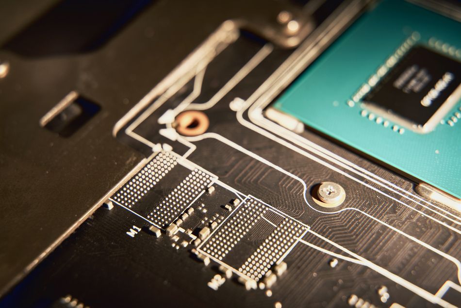
GDDR6 Specifications and Architecture
GDDR6 memory, standardized by JEDEC in July 2017, began mass production in 2018 under JESD250, and is the baseline high-performance graphics memory standard used across the majority of discrete GPUs sold today.
Data Rate and Bus Organization
GDDR6 uses NRZ signaling, where each symbol represents a binary 0 or 1. The Micron GDDR6 flyer specifies data rates up to 16 Gb/s per pin with 32 DQ lines organized as two 16-bit channels [1]. High-performance variants from Samsung and SK hynix push up to 18 Gb/s, and Samsung's 24 Gb/s GDDR6 devices use GDDR6 devices use advanced process technologies. [5].
Each GDDR6 device typically has an 8 GB or 16 GB die. Modules connect to GPUs via 256-bit or 384-bit buses. The RTX 4090 uses 24 GB of GDDR6X (a GDDR6 derivative) on a 384-bit interface, delivering 1008 GB/s of memory bandwidth [7]. The RX 7900 XTX pairs 20 Gb/s GDDR6 with a 384-bit bus for 960 GB/s [7].
Voltage and Power Characteristics
Standard GDDR6 operates at 1.35 V. Some lower-power modules run at 1.25 V. Direct energy-per-bit comparisons between GDDR6 and GDDR6X vary by implementation and are not consistently standardized across vendors. Voltage scaling below 1.35 V is possible but may limit data rates. Vendors such as Samsung offer low-power GDDR6 at 1.1 V for mobile graphics, or low-power uses [5].
Dual-Channel Architecture
Each GDDR6 device contains two independent 16-bit channels (or four 8-bit sub-channels) with a 2-channel 32-byte access granularity [1]. This allows the memory controller to issue commands to one channel while the other returns data, reducing bank conflicts and improving efficiency.
GDDR6X Variant
GDDR6X, developed by NVIDIA and Micron, pushes beyond 19 Gb/s per pin using PAM4. PAM4 encodes 2 bits per symbol through four voltage levels but suffers from reduced signal margin. GDDR6X memory on the RTX 4090 runs at 21 Gb/s, delivering 1008 GB/s on a 384-bit bus [7]. PAM4's complexity increases dynamic current draw and requires advanced equalization, which is why GDDR6X is primarily used in high-end GPUs due to power, signal integrity, and design complexity considerations.
Recommended Reading: GDDR6 vs GDDR6X: A Comprehensive Technical Comparison for Digital Design & Hardware Engineers
GDDR7 Specifications and Architecture
The GDDR7 specification (JESD239) aims to double the performance of GDDR6 while improving power efficiency and reliability.
Data Rate and Bandwidth
Initial GDDR7 devices deliver 32 Gb/s per pin with a roadmap to 48 Gb/s [3]. At 32 Gb/s on a 32-bit device, this equates to 128 GB/s bandwidth per chip. At 48 Gb/s, the per-device bandwidth reaches 192 GB/s [4]. Since GPUs typically connect multiple memory chips in parallel, a 256-bit interface yields 1 TB/s at 32 Gb/s and 1.5 TB/s at 48 Gb/s. Micron reports a system bandwidth of 1.5 TB/s on its early GDDR7 samples [1].
PAM3 Signaling
GDDR7 transitions from NRZ/PAM4 to PAM3. In PAM3, three voltage levels encode about 3 bits over two cycles, increasing throughput without doubling the number of voltage levels [3]. Each clock cycle transmits 50% more information than NRZ, but with better signal margins than PAM4. The Rambus specification notes that PAM3 reduces voltage swing and improves tolerance to noise and crosstalk [3].
Channel Architecture and Density
GDDR7 devices feature four independent 8-bit channels rather than two 16-bit channels [3]. This finer granularity allows memory controllers to schedule more concurrent transactions and reduces access latency. The standard supports densities from 16 GB to 32 GB per die, enabling 2 GB to 4 GB per chip. On-die error correction and data poisoning detection further enhance reliability [4].
Voltage and Power Efficiency
To support higher data rates without excessive heat, GDDR7 lowers operating voltage to 1.1-1.2 V [3]. TrendForce reports that SK hynix's GDDR7 achieves a 40% improvement in power efficiency, and that Micron's early devices offer up to 50% energy efficiency improvement and a 70% reduction in standby power via a new sleep mode [6]. The reduction in voltage and more efficient signaling are key for AI workloads that scale memory bandwidth linearly with performance.
Vendor Implementations
Micron's first GDDR7 samples operate at 32 Gb/s on a 1β (1-beta) process technology [1]. Samsung announced 16 GB GDDR7 chips achieving 32-40 Gb/s at 1.1 V and hints at 48 Gb/s variants. SK hynix demonstrates 16 GB and 24 GB GDDR7 devices running at 40 Gb/s with 160 GB/s bandwidth per chip.
Recommended Reading: What is High Bandwidth Memory 3 (HBM3): Complete Engineering Guide 2025
Head-to-Head Comparison
The following table summarizes the key differences between GDDR6, GDDR6X, and GDDR7. Numbers represent typical or specified values. Actual products may vary.
Attribute | GDDR6 | GDDR6X | GDDR7 |
Per-pin data rate | 14-18 Gb/s (up to 24 Gb/s in Samsung high-K devices) [1][5] | 19-24 Gb/s (21 Gb/s on RTX 4090) [2][7] | 32-48 Gb/s [3] |
Channel architecture | Two 16-bit channels (x16/x8) [1] | Two 16-bit channels | Four 8-bit channels [3] |
Signal encoding | NRZ (PAM2) | PAM4 (2 bits per symbol) [2] | PAM3 (~1.58 bits per symbol) [3] |
Nominal voltage | 1.35 V (1.25 V variants) [1] | ~1.35 V | 1.1-1.2 V [3] |
Die capacities | 8 -16 GB [1] | 8 -16 GB | 16 -32 GB [4] |
Per-device bandwidth | ~64-96 GB/s (16 Gb at 16 Gb/s) | ~96-128 GB/s (21 Gb/s) | 128 GB/s (32 Gb/s) to 192 GB/s (48 Gb/s) [4] |
Notable GPUs | RX 7900 XTX (20 Gb/s) [7], RTX 4080, RTX 4070 (GDDR6 variant, 20 Gb/s — introduced August 2024) | RTX 3080 and RTX 3090, RTX 4090 (19-21 Gb/s), RTX 4070 original (21 Gb/s) [7] | Next-generation GPUs (e.g., RTX 50-series, RDNA 4) are expected to adopt GDDR7. |
PAM3 vs NRZ vs PAM4 Signaling
Memory signaling technology is critical because it defines how many bits of data can be transmitted per symbol period.
NRZ
NRZ (Non-Return-to-Zero) is the simplest form of line coding, using just two voltage levels — +V for a logic 1 and −V for a logic 0. The signal holds its level for the entire symbol period, transitioning only when the bit value changes, which means one symbol carries exactly one bit of information.
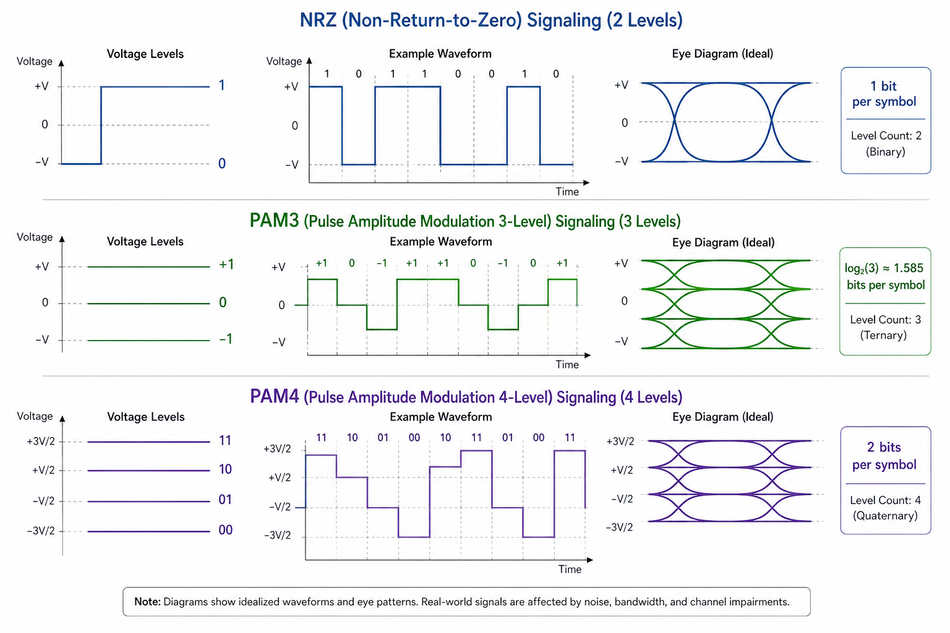
PAM4
PAM4 (Pulse Amplitude Modulation with four levels) encodes 2 bits per symbol using four voltage levels. Doubling the bits per symbol increases throughput without doubling the clock frequency, but the voltage margin between levels decreases. This makes PAM4 signals more susceptible to noise and requires complex equalization and error correction. GDDR6X adopts PAM4 to achieve 19–21 Gb/s per pin at the cost of higher dynamic power consumption. [2].
PAM3
PAM3 introduces three discrete voltage levels and encodes approximately 1.58 bits per symbol [3]. It does not provide as much throughput per symbol as PAM4, but the reduced number of levels improves signal integrity and noise tolerance. Rambus notes that PAM3 used in GDDR7 transmits 3 bits over two cycles — 50% more data at an identical clock frequency than NRZ — while requiring less voltage headroom than PAM4 [3].
Current Generation GPUs (2022–2024)
NVIDIA GeForce RTX 4090. The flagship Ada Lovelace GPU uses GDDR6X memory. According to PNY's specification sheet, it runs at 21 Gb/s with a 384-bit interface and supplies 1008 GB/s of bandwidth [7]. This bandwidth supports 4K gaming and AI workloads.
AMD Radeon RX 7900 XTX. AMD's RDNA 3 flagship pairs 24 GB of 20 Gb/s GDDR6 with a 384-bit bus for 960 GB/s of raw bandwidth [7]. AMD complements the memory with 96 MB of Infinity Cache, with AMD claiming an effective bandwidth of up to 3,500 GB/s under ideal cache hit conditions [7].
Early GDDR7 GPUs (2025 onward)
NVIDIA RTX 5080 and RTX 5090. The RTX 5080 uses 30 Gb/s GDDR7 on a 256-bit bus, delivering 960 GB/s of memory bandwidth [5]. The RTX 5090, based on the Blackwell architecture, uses 28 Gb/s GDDR7 on a wider 512-bit bus, delivering 1,792 GB/s — nearly double the RTX 4090's bandwidth [5].
SK hynix demo and roadmap. SK hynix demonstrated 16 Gb and 24 Gb GDDR7 chips running at 40 Gb/s, with a per-chip bandwidth of 160 GB/s, and mass production began in Q1 2025 [8]. These modules will enable GPUs to exceed 1.28 TB/s of memory bandwidth on a 256-bit bus.
RDNA 4. AMD's current RDNA 4 lineup, which launched in March 2025, uses GDDR6 with an improved memory compression pipeline [9]. The RX 9070 XT uses 20 Gb/s GDDR6 on a 256-bit interface with 16 GB of memory, balancing bandwidth and cost.
Workstation and AI accelerators. Professional GPUs such as the RTX 6000 Ada and A100 rely on HBM rather than GDDR. Lower-end workstations may adopt GDDR7 to deliver near-HBM bandwidth at lower cost. The improved efficiency and higher densities of GDDR7 also make it attractive for AI inference cards that must fit within PCIe power envelopes.
Thermal, Power, and Cost Tradeoffs
Energy Efficiency
The efficiency gap between generations is significant and well-documented by vendors. GDDR6X consumes approximately 15% less power per bit than GDDR6, despite its higher absolute power draw, because PAM4 requires fewer clock cycles to transfer the same data volume — though the increased dynamic current from more frequent transitions narrows this advantage under sustained load.
GDDR7 makes a more decisive break. Samsung claims a 20% improvement in active power efficiency over its own 24 Gb/s GDDR6 implementation, while SK hynix reports over 50% improvement — a wide spread that reflects different measurement methodologies and reference points rather than a contradiction. Samsung separately reports a 50% reduction in standby power consumption, driven by a low-power clocking design. The lower operating voltage of 1.2 V versus GDDR6's 1.35 V accounts for a meaningful portion of these gains, since dynamic power scales with the square of voltage.
Thermal Considerations
Higher data rates generate more heat through switching losses and I/O driver power. GDDR6X modules on cards like the RTX 4090 frequently run at the thermal limit under sustained workloads, requiring integrated thermal pads and direct airflow across the memory packages.
GDDR7 addresses this through both electrical and packaging improvements. SK hynix increased the number of heat-dissipating substrate layers from four to six and used Epoxy Molding Compound to reduce thermal resistance by 74%, without changing module dimensions. Samsung similarly reports a 70% reduction in thermal resistance through new package materials and optimized circuit design. This matters practically — lower memory temperatures under sustained load reduce throttling risk and extend component longevity. Efficient VRM design remains essential to fully realize GDDR7's performance ceiling.
Cost and Availability
GDDR6 remains the most cost-effective option by a wide margin, backed by years of mature production across all three major vendors. GDDR6X carries a premium due to its proprietary PAM4 implementation developed exclusively by Micron for Nvidia — no other vendor produces it, and no JEDEC standard governs it, which limits supply flexibility.
GDDR7 entered mass production in late 2024, with Samsung supplying Nvidia's initial RTX 50 series launch, and SK hynix added as a second source by early 2025. Micron is also sampling GDDR7 on its 1β process node. Early GDDR7 devices are concentrated in high-end GPUs, and mainstream adoption depends on 32 GB die availability, reducing per-gigabyte cost. The added die area from on-die ECC and PAM3 transceiver circuitry pushes GDDR7 costs higher than baseline GDDR6, but the efficiency gains may offset system-level costs through reduced cooling overhead.
Future Outlook
JEDEC has a consistent pattern of mid-generation derivatives — GDDR5X and GDDR6X both followed this model. SK hynix presented a research paper at ISSCC 2026 demonstrating 48 Gb/s operation at 24 Gb density, representing over a 70% speed increase over the current 28Gb/s density. Whether this becomes a formal GDDR7X standard or simply an extension of JESD239 remains to be seen.
Longer term, CXL-attached memory and 3D-stacked DRAM architectures could challenge GDDR's position in workloads where latency and capacity matter as much as bandwidth. For the near future, GDDR7 anchors high-end and eventually mainstream discrete GPUs, HBM remains exclusive to data-center accelerators where cost-per-bandwidth-per-watt justifies it, and GDDR6 continues serving budget and midrange designs where its maturity and pricing are unmatched.
Conclusion
GDDR7 represents a significant step forward in graphics memory. By moving to PAM3 signaling, doubling the number of independent channels from two to four at 8 bits each, and reducing operating voltage to 1.2 V, it doubles per-device bandwidth relative to GDDR6 and offers superior energy efficiency [3]. Shipping implementations run at 28–30 Gb/s per pin, with the RTX 5080 delivering 960 GB/s on a 256-bit bus and the RTX 5090 reaching 1,792 GB/s on a 512-bit bus [5]. GDDR6 continues to deliver strong performance for current high-end GPUs and remains cost-effective for mainstream parts. GDDR6X's PAM4 approach provides higher bandwidth than GDDR6 but consumes more power and is limited to select products [2].
Engineers and informed consumers should weigh memory bandwidth, power draw, and cost when selecting a GPU. For gaming at 4K or AI inference workloads requiring large parameter sets, GDDR7 offers the best balance of bandwidth and efficiency. For midrange builds, GDDR6 still suffices and benefits from widespread availability.
With GDDR7 now in mass production and Nvidia's RTX 50 series and AMD's RDNA 4 both shipping, the transition to PAM3-based memory is already underway. Future memory standards will likely continue pushing signaling rates or adopt alternative interconnects to meet sustained demand for bandwidth.
FAQ
What is the difference between GDDR6 and GDDR7 memory?
GDDR6 uses NRZ signaling and operates at 14-18 Gb/s per pin with 1.35 V [1]. GDDR7 introduces PAM3 signaling, enabling 32-48 Gb/s per pin at 1.1-1.2 V [3]. It also features four 8-bit channels (versus two 16-bit channels) and on-die ECC. These changes double per-device bandwidth and reduce power consumption.
Is GDDR7 faster than GDDR6X?
GDDR6X uses PAM4 to reach 19-21 Gb/s per pin [2]. Early GDDR7 devices operate at 32 Gb/s with a roadmap to 48 Gb/s [3]. GDDR7 surpasses GDDR6X in maximum data rate and does so with better energy efficiency thanks to lower voltage and fewer signaling levels. Actual performance still depends on the GPU's memory controller and bus width.
Which GPUs currently use GDDR7 memory?
As of early 2026, Nvidia's GeForce RTX 5080 uses 30 Gb/s GDDR7, and the RTX 5090 and other RTX 50-series cards use 28 Gb/s modules [5]. All three major vendors — Samsung, Micron, and SK hynix — are in mass production, with devices running at 32–40 Gb/s available for integration into next-generation GPU designs.
How does PAM3 compare to PAM4 in memory signaling?
PAM4 encodes 2 bits per symbol using four voltage levels but suffers from reduced voltage margin and higher noise susceptibility [2]. PAM3 uses three voltage levels to encode roughly 3 bits over two cycles. [3]. This design delivers 50% more data per clock than NRZ while maintaining better signal integrity than PAM4. PAM3 provides a sweet spot between throughput and reliability for GDDR7.
Will older GPUs support GDDR7?
No. GDDR7 requires a memory controller designed for PAM3 signaling and four 8-bit channels. Existing GPUs with GDDR6 or GDDR6X controllers cannot be retrofitted. Only new graphics processors manufactured with GDDR7-compatible memory interfaces will use this memory standard.
How does memory bandwidth influence gaming and AI performance?
Memory bandwidth determines how quickly data reaches the GPU cores. High-resolution textures, ray tracing, and AI inference require moving large amounts of data rapidly. Insufficient bandwidth causes shader stalls and reduces frame rates. Upgrading from GDDR6 to GDDR7 can increase effective bandwidth by up to 2×, improving performance in bandwidth-sensitive workloads.
What are the power requirements for GDDR7 memory?
GDDR7 operates at 1.2 V, lower than the 1.35 V used by GDDR6 [3]. Samsung reports a 20% improvement in active power efficiency over GDDR6 and a 50% reduction in standby power consumption. SK hynix claims over 50% improvement in power efficiency. The 70% figure sometimes cited refers to a reduction in thermal resistance through new packaging materials, not standby power [6]. These gains allow GPUs using GDDR7 to deliver higher bandwidth without proportionally increasing board power.
When will GDDR7 become mainstream?
Samsung and Micron entered mass production in Q4 2024, with SK hynix following in Q1 2025 [8]. High-end adoption is already underway with the RTX 50 series. As 32 GB die densities become widely available and per-unit costs fall, GDDR7 is expected to reach midrange GPUs by 2026–2027.
References
[1] Micron Technology, “GDDR6 SDRAM,”
Available: Link
[2] Wevolver, “GDDR6 vs GDDR6X: Differences Explained,”
Available: Link
[3] Rambus, “All You Need to Know About GDDR7,”
Available: Link
[4] JEDEC, “JEDEC Announces GDDR7 Memory Standard (JESD239),”
Available: Link
[5] Wccftech, “Samsung’s 24 GB GDDR7 Memory Can Pave The Way For Higher-Capacity Consumer GPUs, Up To 42.5 Gbps Speeds”
Available: Link
[6] TrendForce, “GDDR7 Emerging as a New Driver for Memory Industry”
Available: Link
[7] PNY Technologies, “GeForce RTX 4090 24GB,”
Available: Link,”
[8] KitGuru, “SK hynix Shows Off GDDR7 Memory Running at 40Gbps,”
Available: Link
[9] Hot Chips 2025, “Hot Chips 2025 Conference Program,”
Available: Link