Double-Pulse Testing for Power Semiconductor Devices with Infineon's EVAL-DCLINK-DPT Evaluation Board
Infineon's EVAL-DCLINK-DPT is used to perform double pulse testing for high-voltage power devices to evaluate switching losses, turn-on and turn-off behavior, reverse recovery, gate waveform integrity, parasitic effects, and safe operating margins under defined voltage and current conditions.

30 Mar, 2026. 7 minutes read
Introduction
With the recent surge in industrial and household power demands driven by factors like AI, electrification, and automation, power electronic converters are required to operate at higher voltages, higher switching speeds, and tighter efficiency margins. During the product design cycle, engineers must thoroughly understand the behavior of the power switches to be able to build products that meet such performance and efficiency expectations.
This article explains double-pulse testing (DPT), a practical, widely used method for characterizing the switching behavior of power semiconductor devices. It presents Infineon’s EVAL-DCLINK-DPT board as a platform for early-stage design validation.
Double Pulse Testing in Practice: What Is Measured and Why
DPT is a controlled switching experiment used by engineers to observe a power switch’s dynamic behavior under realistic electrical stress. A typical DPT setup consists of the following elements:
DC-link capacitor network: Provides a stable DC bus that minimizes parasitic inductance that could distort switching waveforms.
Device under test (DUT): The power semiconductor device under test in a half-bridge configuration.
Load inductor: An inductor to set and control the current level during the first pulse and put a limit on di/dt to maintain controlled test conditions.
Gate driver: Necessary for providing switching signals and controlling the switching of the DUT.
Double-pulse generator: Generates a pulse with a specific timing, duration, and repetition to enable consistent and repeatable switching events.
High-voltage DC power supply: An adjustable source of power that can be set at different voltage levels to understand how the switch behaves at different operating conditions.
Measurement and probing equipment: High-voltage differential probes, current sensors, and oscilloscopes to capture waveforms with sufficient bandwidth and high accuracy.
A DUT is configured in a half-bridge setup, which is subjected to two gate pulses separated by an interval of defined off-time. When the first pulse is triggered, it establishes a known current through the device and load inductor. The second pulse forces the device to switch at that controlled current level, letting engineers measure the device’s dynamic behavior under realistic electrical stress conditions.
This approach helps engineers evaluate parameters, such as:
Turn-on and turn-off behavior, including switching speed and waveform shape
Switching energy losses, which directly affect efficiency and thermal design
Voltage overshoot and ringing, often driven by parasitic inductance in the commutation loop
Current transients and reverse recovery effects (more relevant in complementary devices or diodes)
DPT is typically performed before a full power converter prototype is built. This lets engineers evaluate the power stage in isolation without worrying about the complex system where multiple variables interact. This simplifies the development and reduces the likelihood of unexpected issues at a later design stage.
The Role of the DC-Link in Accurate Double Pulse Testing
During a DPT, the DC-link is an important element that determines how accurate and repeatable the test results will be. Beyond a voltage source, it is a part of the switching loop. Its impedance, layout, interconnection quality, and other features directly influence voltage overshoots, ringing behavior, and switching losses.
During high-speed switching, the current commutates rapidly through the circuit. Any stray inductance in the path generates additional voltage proportional to di/dt. For high-speed switching circuits using SiC devices, di/dt can reach high values, and even small parasitic inductances in the DC-link can produce large voltage overshoot. If not managed properly, it can artificially inflate measured switching stress, distort waveforms, push the DUT beyond its safe limits, or introduce more ringing and make loss calculation more difficult.
Similarly, poorly placed decoupling capacitance allows DC bus voltage to dip during long current pulses. This voltage changes switching conditions and makes measurements inaccurate.
The DC-link must also be mechanically robust and have strong and optimized electrical connections to reduce variability between test setups. Finally, the circuit must provide a controlled discharge behavior to ensure the safety and repeatability of the test results.
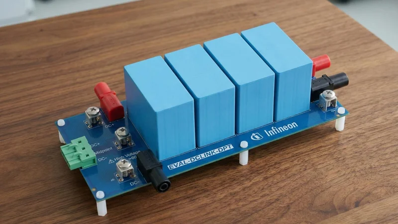
Infineon EVAL-DCLINK-DPT Evaluation Board
Infineon’s EVAL-DCLINK-DPT Evaluation Board is a dedicated DC-link platform for performing DPT on power switches with outstanding accuracy. It provides a stable DC bus, capacitor network, and controlled interconnection platform that DPT requires.

The kit connects with compatible plug-in DUT boards featuring Infineon’s EiceDRIVER™ gate driver ICs and CoolSiC™ MOSFETs, enabling engineers to evaluate different driver and device combinations during early-stage design. EVAL-DCLINK-DPT comes in a compact form factor of 220 × 120 × 50 mm and is intended for non-continuous lab evaluation uses like DPT, where switching events are short and separated by cooling periods.
Board Architecture and Key Design Features
Infineon EVAL-DCLINK-DPT, at a very high level, can be understood as comprising the following functional sections:
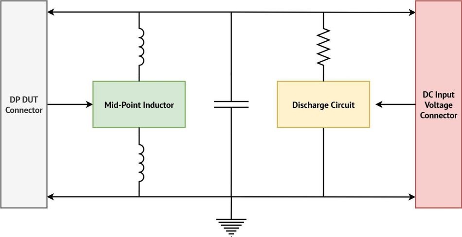
DC Input section
Dedicated high-voltage DC input terminals that allow connection to an external lab power supply operating up to 800 V on the DC-link. This supports realistic stress testing of 1200 V class devices.
DC-Link Capacitor Network
The board includes a capacitor bank to form a DC link. It acts like an energy reservoir to stabilize the bus during transient events. Integrating this network directly on board minimizes interconnection length and reduces stray inductances.
DUT Interface
The board includes a dedicated connector interface that lets users implement a half-bridge configuration with discrete CoolSiC™ MOSFETs, driven by EiceDRIVER™ gate driver circuitry.
Load Inductor Breakout
Dedicated connection points to allow the inductor load to be connected to the setup that controls current during the first pulse and di/dt during switching events.
Active Discharge Circuit
During DPT, a substantial amount of energy is stored in the DC-link capacitor network, which remains there even after the external high-voltage power supply is turned off. This stored energy, if not discharged properly, may pose a safety risk and affect the quality of subsequent tests. To prevent this, EVAL-DCLINK-DPT includes an active discharge circuit that automatically dissipates the residual energy stored in the capacitors once the main supply is turned off.
Visual Safety Features
When the DC-link voltage rises above 60V, a high-voltage LED indicator turns on to enhance user awareness. All the connection points and test points are clearly marked on the board to make things more systematic and organized.
Interfacing with Double Pulse DUT Boards
One of the key features of Infineon EVAL-DCLINK-DPT is its modularity and interconnectability. Instead of having power devices embedded in the circuit, it connects to separate plug-in double-pulse DUT boards that allow users to test out a number of different configurations.
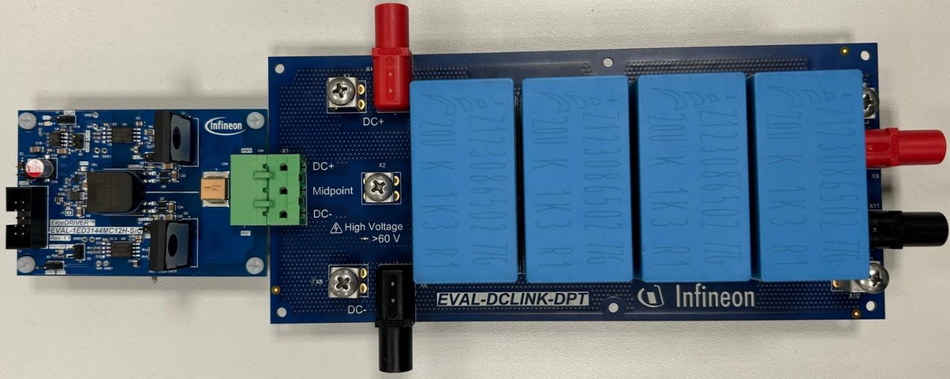
Users can connect EiceDRIVER™ ICs as gate drivers to evaluate the performance of different CoolSiC™ MOSFETs without altering the structure of the DC link itself. This simplifies the evaluation process while avoiding the costs of using a different DC-link for each test.
Supporting Accurate Measurement and Repeatability
During DPT, even small variations in layout, grounding, and probing can influence the switching waveforms. EVAL-DCLINK-DPT supports accurate and repeatable measurements by offering the following features:
Four-Layer PCB Construction
The board comes in a four-layer PCB with 70 µm copper layer thickness. This construction supports high current pulse handling during switching, reduced resistance, and improved thermals. The multilayer construction better separates power and signal paths to reduce coupling effects.
Defined Test Points for Debugging and Analysis
The Infineon EVAL-DCLINK-DPT board comes with several test points for providing access to:
DC input voltage
DC-link positive voltage
Ground references
Discharge MOSFET gate signals
Auxiliary supply nodes
Instead of looking for places to attach probes to bus bars or component leads, engineers can use known reference points designed on the module. These nodes can be used to capture waveforms and for rapid debugging.
Repeatability Across Device Variants
The most fundamental purpose of an evaluation board is to let engineers test out and compare the performance of different configurations and DUTs. With a centralized capacitor network, high-voltage routing, and a discharge circuit, the EVAL-DCLINK-DPT board ensures the circuit returns to the initial state and previous measurements do not influence subsequent tests. This is also a useful feature for safety reasons.
Pairing with EiceDRIVER™ Gate Driver ICs
During DPT, the power device may be the one getting evaluated, but the waveform structures are strongly affected by gate driver performance. During the switching event, the gate driver determines:
Gate voltage amplitude and stability
Rise and fall times of the gate signal
Peak gate current capability
Immunity to high dv/dt disturbances
Ability to avoid parasitic turn-on in the complementary device
In high-voltage SiC-based setups, dv/dt can be steep. If the gate driver lacks sufficient isolation, robustness, or control, it could result in an unintended switching event. For this reason, Infineon’s separate plug-in DUT boards feature gate driver circuitry based on Infineon EiceDRIVER™.

By using purpose-built drivers for fast, high-voltage applications, engineers can make sure the DUT is fully under control.
Evaluating CoolSiC™ SiC Trench MOSFETs
Compared to traditional MOSFETs and IGBTs, wide-bandgap power devices offer faster switching, lower switching losses, and higher voltage levels. The higher performance and efficiency of the devices makes a thorough evaluation mandatory.

Typical Applications and Design Scenarios
Infineon’s EVAL-DCLINK-DPT board offers a convenient and highly accurate way of performing DPT during the design stage for several high-power applications, including the following:
Motor Drives
Fast-switching SiC MOSFETs improve the efficiency of motor drives and reduce the power converter size. However, the switching behavior affects the motor insulation stress, EMI behavior, and various performance parameters of the motors. Performing DPT with EVAL-DCLINK-DPT lets engineers make choices to balance efficiency with robustness.
Electric Vehicles
Onboard chargers and traction converters use MOSFETs with voltage ratings up to 1200 V, which must deliver high efficiency within tight thermal limits. Losses during switching, voltage overshoots, and gate control strategy all affect system size, cooling requirements, and reliability. Performing DPT makes choosing power switches easier.
Renewable Energy
For renewable energy applications, engineers need to ensure stability while operating under varying load conditions. The power switch and gate drive strategy must be tested to make sure the efficiency and performance targets are met by the designs.
Education
The platform is also well suited for academic and research purposes, as engineering students extensively study wide-bandgap device behavior and gate drive strategies. Having a structured framework to conduct DPTs helps students understand real-world power electronics challenges in a safe and controlled laboratory setting.
Conclusion
Accurate characterization of power devices is the first step to designing a high-performance, efficient, and reliable power converter. A loosely assembled test setup may introduce parasitics and variability that could adversely affect the evaluation process for the power devices.
The Infineon EVAL-DCLINK-DPT Evaluation Board ensures the test infrastructure remains constant throughout the iterative testing process. Engineers can perform DPT with different devices and driver combinations under constant DC-link conditions.
Engineers evaluating high-voltage power semiconductor devices can explore more about the Infineon EVAL-DCLINK-DPT Evaluation Board, available through Mouser Electronics.
References
[1] Levett D, Zheng Z, Frank T. Double pulse testing: the how, what and why. Bodo’s Power Systems. 2020 Apr; 30-35. Available from: https://www.infineon.com/assets/row/public/documents/60/54/infineon-double-pulse-testing-bodos-power-systems-article-en.pdf