Chips and Wafers: What's the Difference?
Chips and wafers are the integral components of a semiconductor device. Find out the differences between chip wafers and chips and understand their role in semiconductor manufacturing.

Last updated on 21 Feb, 2024. 9 minutes read
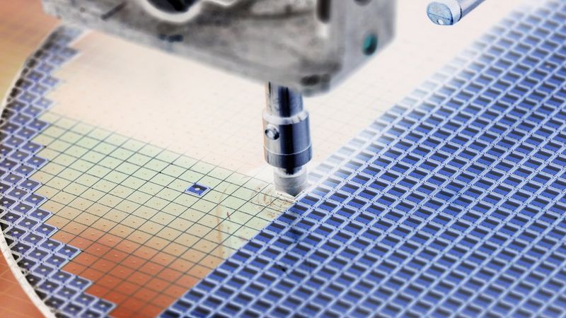
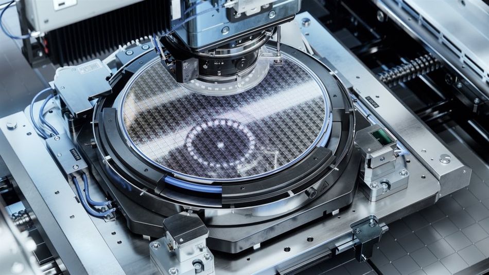
A close-up of a silicon wafer during semi-conductor manufacturing
Introduction
Semiconductor manufacturing is a complex process involving the creation of integrated circuits (ICs) used in electronic devices. It’s a fundamental process for the production of modern technological devices, from smartphones and computers to cars and medical devices. Semiconductors have a higher electrical conductivity than insulators but lower than pure conductors. Silicon is an essential semiconductor material used in the manufacturing of these semiconductor devices.
The manufacturing begins with silicon chip wafers, the thin slices of silicon crystal. These wafers serve as the substrate for the IC. Later, the chip wafers undergo various processes, such as doping, oxidation, and lithography, to create the IC. While chips and wafers may seem identical, and the term ‘chip wafers’ is often used for micro-level semiconductor devices, some important differences differentiate the two semiconductor materials. This post will discuss the essentials of chip wafers and how they are used in semiconductor manufacturing systems. .
Recommended Reading: How are Semiconductors Made? A Comprehensive Guide to Semiconductor Manufacturing
What are Wafers?
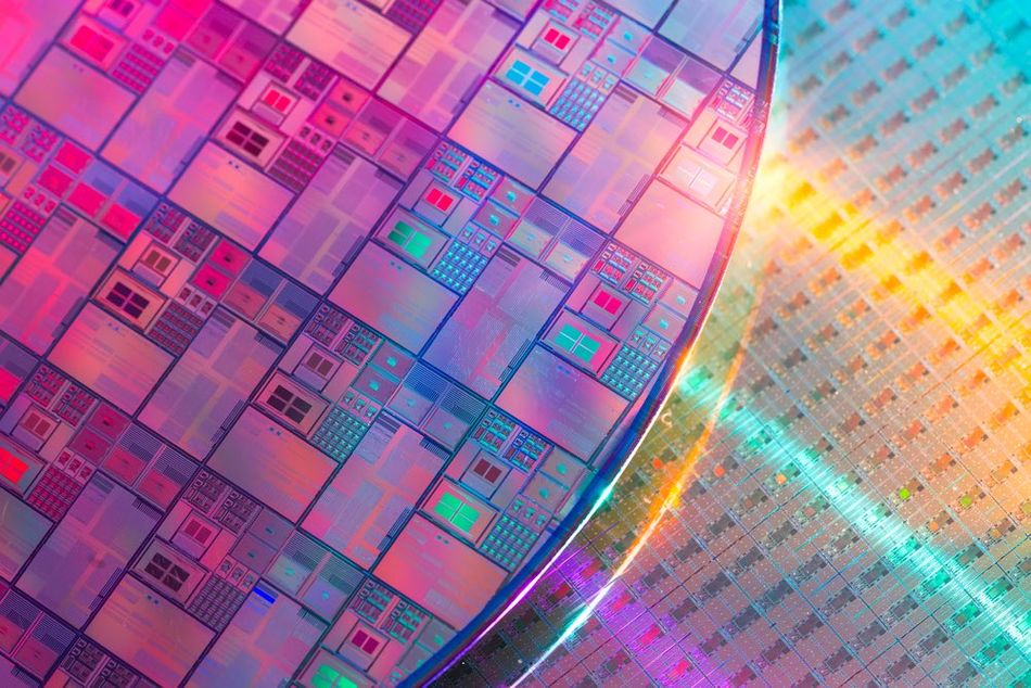
A semiconductor wafer refers to a thin slice of semiconductor material, usually crystalline silicon obtained from sand (Silica) used as the substrate for microelectronic devices like integrated circuits (ICs) and microchips, etc. Typically, the wafers are circular shaped, ranging in diameters from a few millimetres to several inches. Later, the silica is reduced to pure silicon through a series of chemical reactions.
Wafer Diameter and Thickness
Wafers are characterized by their diameter and thickness. The diameter of wafers has steadily increased over the years to improve productivity and reduce cost per chip. Currently, the standard wafer diameter is 300mm, or about 12 inches, although 450mm wafers are in development. The thickness of the wafer is typically a few hundred micrometres.
The surface of the wafer is polished to a mirror finish to remove imperfections that could impact the performance of the microelectronic devices built on it. Moreover, the wafer also needs to be extremely flat to ensure proper photolithography later.
Wafer Purity
The silicon used to make the wafer needs to be 99.9999% pure, a level of purity known as "six nines". Otherwise, impurities could interfere with the operation of the devices built on the wafer.
Wafer Material
The type and materials of wafers can vary greatly, depending on the type of semiconductor device that needs to be produced. Typically, the following materials are used for semiconductor wafer manufacturing:
- Silicon Germanium (SiGe)
- Sapphire (Al2O3)
- Gallium Arsenide (GaAs)
- Gallium Nitride (GaN)
- Diamond
- Zinc Oxide (ZnO)
- Silicon Carbide (SiC)
- Indium Phosphide (InP)
How a Silicon Wafer is Manufactured - The Czochralski Method
Silicon wafers are made from sand through a process called the Czochralski method. The process is named after the Polish scientist Jan Czochralski, who invented the method.
In this process, a small silicon seed crystal is dipped into a molten pool of pure silicon and then slowly pulled out, causing the silicon to crystallize around the seed.
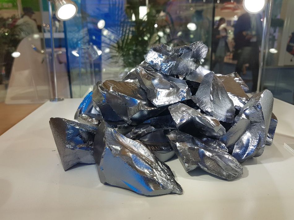
First, high-purity silicon dioxide is extracted from sand and reduced to elemental silicon through a chemical reaction with carbon.
Next, the silicon is melted in a crucible and a seed crystal is dipped in and slowly pulled out, creating a single crystal ingot.
Finally, the ingot is sliced into thin wafers using a diamond saw and undergoes polishing and cleaning to remove imperfections, resulting in the final silicon wafer ready for semiconductor fabrication. The idea is to fabricate a wafer of the desired thickness that can be further used in the manufacturing of semiconductor devices.
Further Reading: Wafer Thinning: Investigating an essential part of semiconductor fabrication
Polishing
After the wafers are cut, they are polished to create a smooth, flat surface, through a a process called chemical-mechanical planarization. It involves grinding and polishing the wafer with a mixture of chemicals and abrasive particles. The result is a mirror-like finish that is necessary for the subsequent processes of semiconductor manufacturing.
Cleaning
The final step in the wafer creation process is cleaning. The wafers are cleaned to remove any residual particles or contaminants that could interfere with the manufacturing process. This is done using a series of chemical baths and rinse cycles.
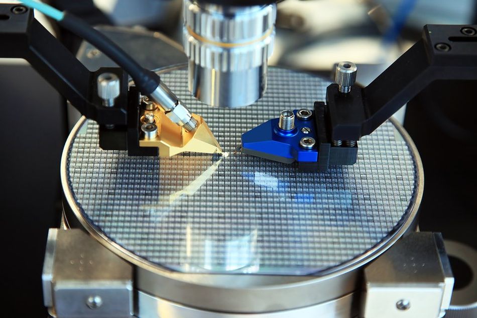
Testing
After preparation, the wafer undergoes a series of processes to create the IC. These processes include oxidation and photolithography, where a pattern of the IC is transferred onto the wafer using light. Later, the patterned wafer undergoes a series of processes such as:
- Etching
- Doping
- Testing
Once tested, the wafer is cut into individual chips, which are packaged and prepared for use in electronic devices.
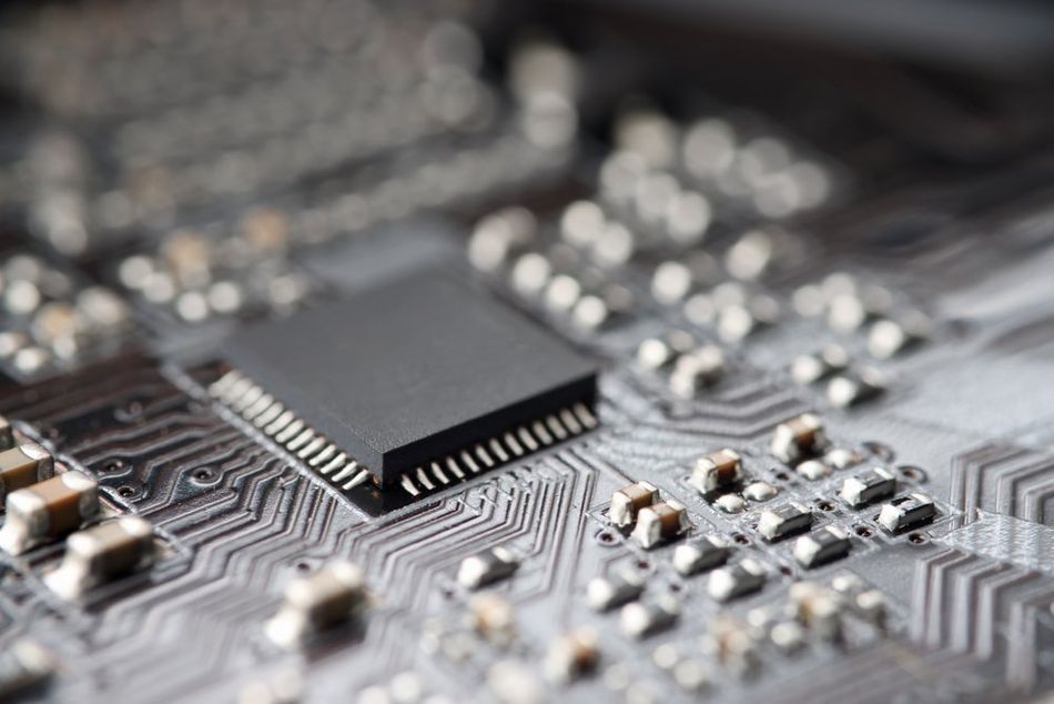
What are Semiconductor Chips?
In semiconductor manufacturing, a chip is also known as an integrated circuit (IC). It is a set of electronic circuits featuring a compact assembly of interconnected components like resistors, transistors, capacitors, etc. on a small flat piece, or "chip", of semiconductor material. These components are etched onto the chip of semiconducting material, such as silicon or germanium.
The electronic circuits on the chip are created by depositing layers of different materials and etching patterns into them. The result is a complex network of interconnected components that can perform various functions.
Chips are characterized by their size, structure, and functionality. The size of a chip is typically measured in millimetres and can vary depending on the complexity of the circuits it contains. For example, a simple logic chip might be just a few millimetres on each side, while a complex microprocessor could be 20mm or more on each side.
Chip Structure
The structure of a chip refers to the arrangement of its internal components. This includes the layout of the circuits and the placement of the transistors, resistors, and capacitors. It must be carefully designed to optimize performance and reduce power consumption.
Functionality
Chip functionality depends on the circuits it contains. Some chips, like memory chips, have a single function, while others, like microprocessors, are multifunctional. The functionality is determined by the design of the circuits and the way they are interconnected.
How a Chip is Manufactured
Chip manufacturing begins after wafer preparation. The wafer serves as the substrate on which the chips are created. Chip creation involves several steps, including photolithography, etching, and doping, which are repeated multiple times to build up the complex structures of the chip.
Photolithography
Photolithography transfers the circuit design onto the wafer. It involves coating the wafer with a light-sensitive material called photoresist. A mask, which is a stencil of the circuit design, is then placed over the wafer, and ultraviolet light is shone onto it. The light hardens the photoresist in the pattern of the circuit design, while the unexposed areas remain soft.
Etching
Etching is the process of removing unwanted material to create the features of the chip by using chemicals that eat away the wafer's exposed areas, leaving behind the desired pattern. It also removes the underlying layers of silicon and other materials in the pattern of the circuit design.
Doping
Doping is the process of changing the properties of the silicon in the wafer to create the different components of the chip. This is done by introducing impurities into the silicon, which changes its conductivity. The type and amount of impurities determine whether the silicon becomes n-type, which has an excess of electrons, or p-type, which has a shortage of electrons. The interaction between n-type and p-type silicon forms the basis of the transistors that make up the circuits on the chip.
The photolithography, etching, and doping processes are repeated multiple times to build up the complex structures of the chip. Each repetition adds a new layer to the chip, with each layer serving a specific function in the final circuit.
Functionality Testing
Once the chip is created, it is tested for functionality and performance. This involves applying electrical signals to the chip and measuring its response. If the chip passes the tests, it is cut from the wafer and packaged for use in electronic devices.
Further Reading: Semiconductor Fabrication Process: The Ultimate Guide to Creating Cutting-Edge Electronics
Key Differences Between Wafers and Chips
While chips and wafers are typically used interchangeably in electronics, there are some notable differences between the two. One of the key differences is that a chip or integrated circuit is an assembly of electronics, while a wafer is a thin slice of silicon that is used for the formation of integrated circuits.
Here are some more important differences between chips and wafers.
Material and Structure
The material and structure are two fundamental differences between chips and wafers. Wafers are thin slices of semiconductor material, typically silicon, and are characterized by various properties such as diameter, thickness, and surface properties, such as flatness and purity.
On the other hand, chips are the functional units of a semiconductor device, consisting of interconnected electronic components that are built on the wafer substrate through a series of complex processes. The structure of a chip is determined by the arrangement of its internal components and the layout of the circuits.
Production Process
The production processes for wafers and chips are distinct, with each requiring specific techniques and equipment to achieve the desired outcome.
Wafer Production Process | Chip Production Process |
Silicon purification: Silicon extraction and purification to achieve 99.9999% purity. | Photolithography: Wafer coating with photoresist, masking, and hardening with ultra-violet light. |
Crystal growth: Silicon boule is created using the Czorchralski method. | Etching: Using chemicals to remove the soft areas of the photoresist. |
Wafer slicing: Slicing the boule into thin wafers with a diamond saw. | Doping: Introducing impurities into silicon to create n-type or p-type materials. |
Wafer polishing: Polishing the wafers to create a mirror-like finish using chemical-mechanical planarization. | Layering: Repeating photolithography, etching, and doping processes multiple times to build up the complex structures of the chip. |
Wafer cleaning: Removing residual particles or contaminants using a series of chemical baths and rinse cycles. | Testing and packaging: Testing for functionality and performance. |
Functionality
Another key difference between wafers and chips is their functionality within the semiconductor manufacturing process.
Wafer Functionality
The primary function of a wafer is to serve as the substrate or base for the fabrication of integrated circuits. Wafers provide a stable, uniform surface on which the intricate patterns of electronic circuits can be built.
They do not have any inherent functionality in terms of electronic performance. Their role is to provide a suitable platform for the creation of chips, which are the functional units of semiconductor devices.
Chip Functionality
The functionality of a chip is determined by the design of its circuits and the way they are interconnected. Chips can be designed for various applications, from simple logic gates to complex microprocessors. The specific functionality of a chip depends on its intended use and the requirements of the device it will be integrated into.
Conclusion
Wafers and chips are interconnected in semiconductor manufacturing. Understanding the interplay between wafers and chips is crucial for optimized semiconductor manufacturing processes. The differences in material composition, structure, production processes, and functionality between wafers and chips highlight their unique roles and the precision required to create the electronic devices that power our modern world.
Frequently Asked Questions (FAQs)
1. What is the typical size of a wafer?
The typical size of a wafer is determined by its diameter, which has increased over the years to improve productivity and reduce cost per chip. The standard wafer diameter is 300mm, or about 12 inches, although 450mm wafers are in development.
2. How many chips can be made from a single wafer?
The number of chips that can be made from a single wafer depends on the size of the chips and the size of the wafer. Larger wafers can yield more chips, while smaller chips allow for more efficient use of the wafer surface. The exact number of chips per wafer varies depending on these factors and the specific manufacturing process used.
3. What materials are used to make wafers and chips?
Wafers are typically made from silicon, which is a semiconductor material. Silicon is used because it can withstand high temperatures, is abundant, and has the right semiconductor properties. Other wafer manufacturing materials include Silicon Germanium (SiGe), Sapphire (Al2O3), Gallium Arsenide (GaAs), Gallium Nitride (GaN), Diamond, Zinc Oxide (ZnO), Silicon Carbide (SiC), and Indium Phosphide (InP). Chips, or integrated circuits, are created on the silicon wafer substrate through a series of complex processes involving various materials, such as metals and insulators, in addition to silicon.
4. Why is silicon commonly used in wafer and chip production?
Silicon is commonly used in wafer and chip production due to its excellent semiconductor properties, ability to withstand high temperatures, and abundance in the earth's crust. These characteristics make silicon an ideal material for creating wafers and chips in the semiconductor manufacturing process.
5. What happens to the wafer after the chips are cut out?
After the chips are cut out from the wafer, the remaining wafer material, known as "wafer scrap," is typically recycled or disposed of according to industry standards and regulations. The cut chips are then packaged and prepared for use in electronic devices.
References
https://www.universitywafer.com/semiconductor-wafer.html
https://semiconwafers.com/si_wafers_properties/properties_of_silicon
https://www.differencebetween.info/difference-between-chip-and-wafer-in-electronics