Be the first to know.
Get our additive electronics  weekly email digest.

Tagged with

Additive Electronics

ORGANIZATIONS. SHAPING THE INDUSTRY.

Latest Posts

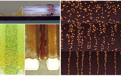
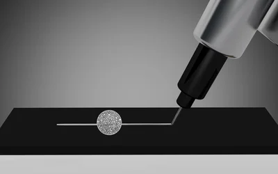
Advanced packaging of semiconductor-based sensors - specially on flexible substrates- brings very specific interconnection requirements. These often are related to a very narrow pitch of the interconnections or the fragility of the sensor. Learn how inkjet printing solves the issues

Inkjet printed wirebonds for sensor interconnections

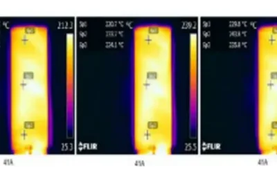
The key enabler for reliable device fabrication in printed electronics is functional inks with tunable electrical properties incl. conductivity, dielectric strength & electrical resistance. Here, you will learn about unique polyimide based pastes able to withstand temperatures up to 300°C.

Innovative High-Temperature Inks for Printed Electronics

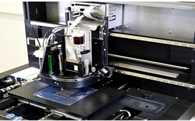
A unique new approach of printing functional materials with unparallel precision and repeatability. Technology called Ultra-Precise Deposition (UPD) is a nanodispensing method capable to print high density and high viscous materials with the resolution down to 1 µm in feature size and with high ratio of width to height after single pass. For this method material extrusion is controlled by a pressure, which means it is not supported with high electric field. Thanks to this there are no limitation if the substrate is conductive or dielectric.

Ultra-Precise Deposition for the Fabrication of Next-Generation MicroLED and QD-LED Displays

The three themes are closely linked since QDs can be digitally printed as color conversation materials atop blue microLEDs to enable wide color gamut RGB uLED displays without requiring a separate transfer step for each color.. This is an important technology as it simplifies the manufacturing step for microLED and thus removing a major hinderence.

The progress of screen printing towards fine line printing has been incredible going from 100 µm features before 2010 to 70 µm to 2015 to 40 µm in 2018 and now pushing - in development- towards 20 µm and less. In parallel, the wet thickness of the printed line have gone down from 12um or so in 2018 to now just 4um.

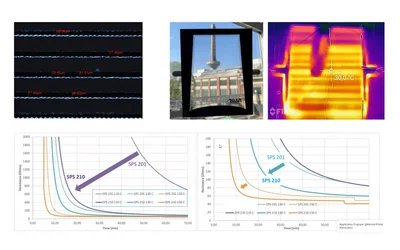
Silver nanoparticle inks improve every year. These improvements are often incremental, but very important. One ever-present direction of development is towards inks which offer ever higher conductivity levels at a low curing temperature and a short curing time. This a critical figure of merit because it opens more substrate choices, saves time, and lowers energy consumption costs.

Ag Nanoparticle Inks: Achieving Ever Higher Conductivity at Lower Curing Time and Temperature