Why 3D IC, Why Now
The Next Wave of Semiconductor Design Complexity

10 Nov, 2026. 5 minutes read
The Strategic Choice Beyond Conventional Scaling
Semiconductor performance has been closely associated with transistor scaling for decades. Smaller process nodes enabled higher transistor densities, shorter interconnects, and greater computational capability within a similar physical footprint. That approach is still important, but the gains available from scaling a single monolithic die are getting harder to achieve without increasing design, power, manufacturing, and cost constraints.
The challenge is not just the number of transistors that can fit onto a chip but how effectively the system uses them. Modern workloads can require high computational throughput, large memory capacity, high memory bandwidth, and rapid movement of data between processing elements. Adding more transistors does not automatically address these system-level requirements.
System-level optimization is therefore an important architectural choice, particularly for artificial intelligence workloads where the relationship between compute, memory, and data movement can influence overall performance. This article discusses how AI workloads are changing semiconductor system requirements, why the industry is turning to 3D IC to address these requirements, and why system-level analysis and connected design workflows are becoming important.
Why AI Workloads Change the Equation
AI workloads are changing what semiconductor systems need from their underlying hardware. Conventional computing involves relatively predictable relationships between processing, memory access, and data movement. AI applications can require substantially higher volumes of computation and data movement, particularly when models contain large numbers of parameters and require repeated data transfer during training. This creates a different system-level constraint.
Moreover, Agentic AI can break a task into multiple steps, invoke different tools or models, retrieve information, and use intermediate results to determine subsequent actions. Each step can involve a different combination of computation, memory access, and data movement, making the workload less uniform and placing different demands on how compute and memory resources communicate.
Therefore, for semiconductor architects, it is important to consider how compute and memory resources are organized and how efficiently they communicate with each other. The question is not only how much computation can be placed on a die, but also how the architecture can organize compute and memory resources to support the required data movement within power, thermal, and physical constraints.
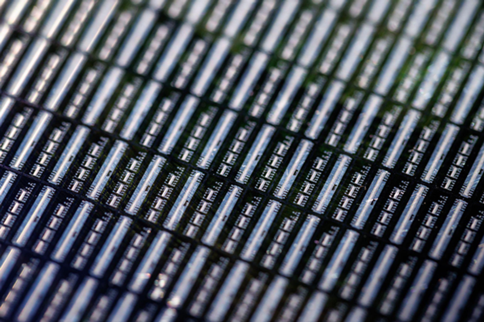 Closeup of microchip circuitry rows on a silicon wafer for semiconductors. Source: AdobeStock.
What Advanced Packaging and 3D IC Enable
Chiplets are another architectural option in which, instead of developing one large die containing every required function, designers can partition a system into smaller dies that perform specific roles and integrate them through suitable interfaces. Heterogeneous integration combines different process technologies, memory types, and functional blocks according to system requirements.
Advanced packaging provides one way to address these architectural requirements by allowing multiple dies and functional blocks to operate as parts of a larger system. Instead of placing every function on one monolithic die, designers can combine components with different characteristics and manufacturing requirements within a common package.
Different packaging approaches provide different trade-offs in density, connectivity, thermal behavior, manufacturing, and cost. For instance, 2.5D approaches can place multiple dies alongside one another on an interposer, creating shorter and wider communication paths between components. Technologies like CoWoS illustrate how this approach can bring high-performance compute components and memory closer together within a package.
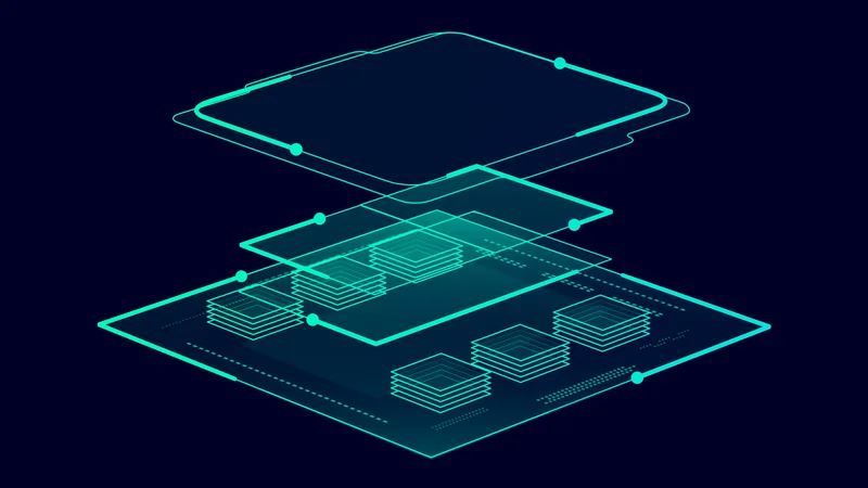
Similarly, 3D IC approaches extend integration even more by stacking components vertically. This can reduce physical distances between functions and increase integration density, although it also introduces additional considerations for thermal management, power delivery, physical reliability, and manufacturing.
The architectural choice is consequently not limited to selecting a process node and designing a die around it. Designers can evaluate how functions should be partitioned, where they should be placed, and how they should communicate as part of the system architecture.
Why Design Complexity Grows Alongside the Opportunity
Greater integration creates opportunities for performance improvements, but it also introduces interactions that are difficult to evaluate within individual design domains.
As industry research highlights, for decades lithography was the primary driver of chip density, but today that has flipped: System Technology Co-Optimization (STCO) now contributes significantly to logic density gains at leading nodes. When leading-edge AI GPUs pack hundreds of billions of transistors and thousands of miles of microscopic copper wiring, resistance and thermal choke points become critical factors. Designers can no longer treat power delivery, signal integrity, and thermal management as separate, sequential steps; they must be evaluated concurrently through an early, system-level design workflow.
Electrical behavior can influence thermal conditions, thermal behavior can affect reliability, and mechanical characteristics can influence the physical integrity of a package and its connections.
These interactions become more important when several dies, interposers, substrates, and interconnect structures are combined. Power delivery should be evaluated across the assembled system instead of only within an individual die. Signal integrity needs to account for the interfaces connecting different components. Thermal analysis needs to consider how heat generated in one region affects neighboring components and the package as a whole. This makes multiphysics analysis an earlier design consideration rather than being treated as a late-stage validation task. Architectural decisions can influence whether a system can meet its power, performance, area, cost, and reliability requirements before detailed implementation begins.
A system-level digital model can provide a way to examine these relationships. In this regard, Siemens Innovator3D IC uses a digital-twin data model for 2.5D and 3D heterogeneous integration, with capabilities for analyzing thermal and electrical characteristics before implementation and verifying system-level functionality and physical interfaces. The value of this approach is not simply that more analysis can be performed. It is that engineering teams can examine the consequences of architectural decisions across the assembled system before those decisions become expensive to change.
The Need for Connected, Automated and Agentic Workflows
The complexity of 3D IC design also changes how engineering teams need to coordinate design activities. A system can involve semiconductor design, package planning, thermal analysis, electrical verification, physical verification, manufacturing, and other disciplines. Decisions made in one domain can create requirements or constraints for another, making isolated workflows difficult to manage as system complexity increases.
Connected workflows can provide a common environment in which information from different stages of the design process can be accessed and evaluated in context. Automation reduces the amount of manual coordination required when engineers need to explore multiple design configurations or repeat analysis across different scenarios.
AI can also support agentic orchestration across engineering workflows. Instead of using AI only to assist with an individual engineering task, agentic systems can coordinate multiple tools and steps according to a defined objective. For instance, Siemens' Fuse EDA AI Agent is designed to orchestrate multi-tool and multi-agent workflows across semiconductor, 3D IC, and PCB system design, including workflows that span design, verification, and manufacturing sign-off.
The objective of agentic orchestration is not to remove engineering decisions, but to give engineers a way to explore, evaluate, and manage those decisions across multiple tools and domains. By connecting specialized engineering capabilities, it reduces the need for each stage to operate as a separate manual workflow. This changes the role of automation from simply executing predefined steps to coordinating engineering activities across a more complex system.
Designing Beyond the Die
3D IC is changing how semiconductor teams approach system architecture. The key question is no longer only how to extract more performance from an individual die, but how to determine the right combination of technologies and integration approaches for a specific system requirement.
For customers building AI-enabled systems, this means making architectural choices at the system level and evaluating them across a broader set of constraints. Decisions about die partitioning, memory, packaging, interconnects, and manufacturing need to be considered in relation to the workloads the system is expected to support. The next stage of semiconductor design will depend not only on advances in individual technologies, but on how effectively those technologies can be brought together and evaluated as a complete system.