The Future of JFETs in a Digital-Dominated World
This article explores the future of JFET technology in a world increasingly defined by sensor proliferation, distributed intelligence, and hybrid analog-digital systems.

09 Jul, 2025. 7 minutes read

Look around, and it’s clear to see that our world is becoming increasingly digitized. The proliferation of sensors, embedded intelligence, and high-speed data processing has created new ways for us to understand and interact with our environment. Yet, the real world is analog, defined by sound, temperature, vibration, light, and pressure. To digitize our world, we must first be able to measure, condition, and translate analog data into digital form. That process begins with precise, low-noise, high-impedance analog circuits.
Among the analog designer’s toolkit, the junction field-effect transistor (JFET) has long held a special place. Although it lacks the ubiquity of CMOS in digital logic or the switching speed of modern MOSFETs, the JFET’s analog characteristics make it indispensable in circuits where signal integrity and noise performance are non-negotiable.
This article explores the future of JFET technology in a world increasingly defined by sensor proliferation, distributed intelligence, and hybrid analog-digital systems.
A Primer on JFETs
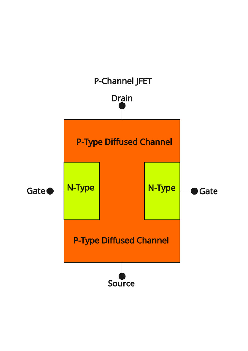
A JFET is a unipolar, voltage-controlled device where current flows through a semiconductor channel that is constricted by a reverse biased p-n junction gate. It is a depletion-mode device, which means it conducts when the gate-source voltage (VGS) is zero and pinches off as VGS becomes increasingly negative (for n-channel types).
The major characteristics that make JFETs attractive for analog designers include
Extremely high input impedance (typically in the teraohm range)
Very low gate leakage current (femtoamp scale)
Low flicker (1/f) and thermal noise
Excellent linearity and thermal stability
Inherently low distortion in small-signal analog regimes
The use of a reverse-biased junction, as opposed to a MOSFET’s insulating gate oxide, is a major benefit of JFETs. This difference in architecture eliminates gate capacitance issues related to charge trapping or oxide breakdown. As a result, JFETs are exceptionally rugged in high-impedance signal paths and low-leakage circuits like precision sensor front ends.
JFETs Enabling Scalable Analog Systems
As the world leans more heavily on digitalization, precision analog circuitry has transcended its confinement to esoteric laboratory equipment or custom aerospace platforms. Today, it is rapidly being integrated into consumer devices, medical wearables, industrial sensors, and IoT edge nodes. And, while sensing becomes decentralized and localized, the front-end requirements of low noise, low power, and minimal parasitic error are increasingly hard to meet with conventional CMOS or bipolar devices alone.
This is where the JFET stands out. In many of these sensor-rich systems, the electrical signals are minute: microvolts of voltage or picoamperes of current. With such amplitudes, any leakage, flicker noise, or thermal drift can bury these signals in distortion.
InterFET and other JFET manufacturers have responded to this challenge with new generations of matched pairs, hybrid-integrated solutions, and custom-fabricated low-capacitance geometries. For example, hybrid assemblies now integrate JFETs with precision passive components and MEMS sensors in multi-chip modules (MCMs), so that designers can build field-deployable, EMI-immune sensing platforms. A complete JFET based analog front end can now fit on a desktop device, a smartwatch, or a sensor pod installed in a wind turbine or remote clinic.
Analog Applications of JFETs
Low-Noise Amplifiers (LNAs)
JFETs continue to define the state of the art in low-noise signal amplification, especially in the audio band and low-frequency domains. Where bipolar transistors suffer from high base current and associated shot noise, JFETs draw almost no gate current. This allows them to amplify signals from sources with extremely high output impedance without adding significant noise.
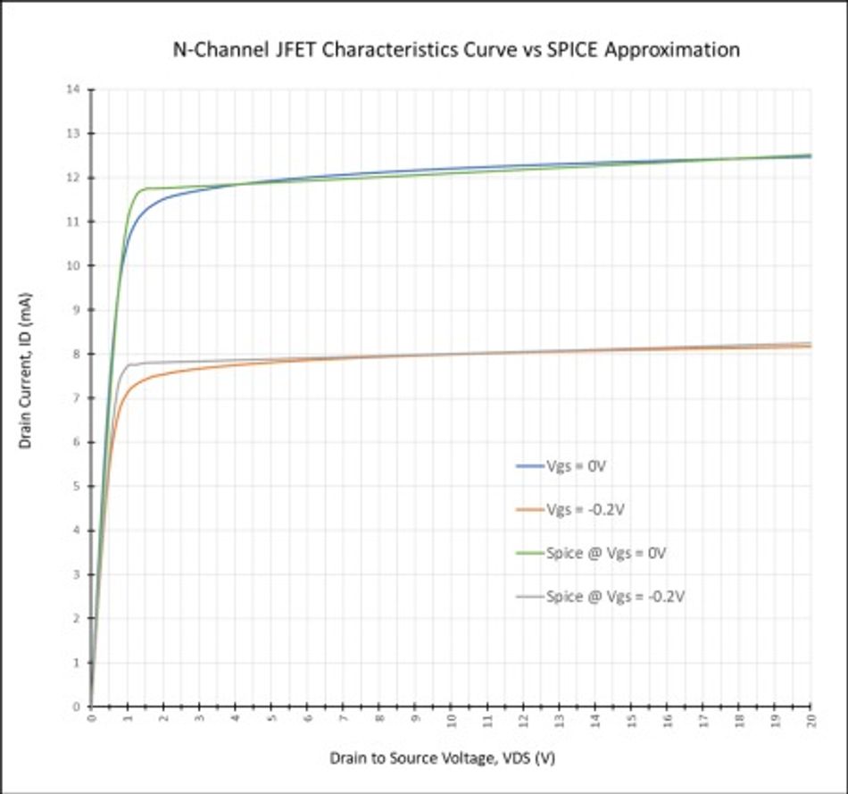
The dominant noise mechanisms in a JFET are thermal channel noise, 1/f flicker noise, and generation-recombination (G-R) noise. These are generally well understood and can be modeled as equivalent voltage and current sources at the gate. Properly biased (typically at VGS ≈ 0 V and ID ≈ 1-3 mA), low-noise JFETs exhibit near-flat noise response up to 100 kHz, with noise figures well below 1 dB.
In applications such as audio preamplifiers and vibration sensors, dual-matched JFETs offer improved common-mode rejection, enabling symmetrical circuit topologies that further reduce intermodulation distortion and thermal drift.
Charge and Sensor Preamps
Many sensors produce charge rather than voltage or current. Examples include piezoelectric accelerometers and capacitive MEMS devices. To convert this charge into a usable voltage without loading the source or distorting the frequency response, analog designers typically use a charge amplifier or transimpedance amplifier (TIA).
The input stage of these amplifiers must have
Very low input capacitance
Extremely high input resistance
Low 1/f and G-R noise
Thermal stability across wide ambient ranges
JFETs meet these demands better than any competing device class. For example, in charge amplifier configurations, JFETs enable stable voltage gain and linear signal conversion when interfacing with capacitive sensors, offering low input capacitance and low noise to preserve signal integrity across a wide dynamic range.
Electret microphones, condenser mic capsules, and infrared pyroelectric sensors are other classic domains where JFET source followers act as impedance converters between a capacitive sensor and a buffered amplifier stage. In these cases, the high input impedance prevents charge loss and preserves low frequency sensitivity.
The Major Growth Drivers for JFET Demand
Individualized Healthcare and Biointerfaces
The convergence of biosensors, wireless communication, and data analytics has created a massive demand for reliable, low-noise analog signal acquisition. Wearable ECG monitors, EEG headsets, and implantable glucose sensors all rely on front ends that can amplify low-amplitude bioelectric signals without compromising signal fidelity.
JFETs’ high impedance and low current noise make them an excellent choice for differential biopotential amplifiers. Their immunity to gate leakage also allows safe interfacing with electrode materials prone to polarization effects.
As medicine shifts from hospital-centered care to continuous, individualized monitoring, analog front ends must also get smaller, quieter, and more energy-efficient. JFETs in hybrid packaging, integrated alongside ADCs and digital radios, will be integral to delivering that capability at scale.
Environmental Sensing and Security
Global instability and the emergence of new threats have also accelerated demand for distributed sensing infrastructure. Whether monitoring for airborne particulates or detecting toxic gas leaks, many of these applications rely on sensors with weak, high-impedance outputs operating in electromagnetically hostile environments.
JFETs, with their ability to operate with high common-mode rejection, low leakage, and low power, are uniquely positioned for applications like gas chromatography, radiation detection, and mass spectrometry
In urban areas, these capabilities are finding their way into smart city infrastructure and airport security scanners, which need miniaturized, autonomous, and reliable analog front ends.
Agriculture and Food Security
In agriculture, the growing use of electrophysiological sensing in plants, soil moisture monitoring, and microbial bio electrochemical systems is creating demand for analog interfaces that work at the edge of detectability.
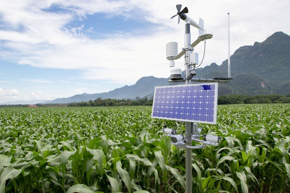
Depleted water tables and harsh soil conditions produce weak and noisy signals, which must be accurately captured to enable automated irrigation or crop health diagnosis. Here again, JFETs provide a low noise, high fidelity bridge between organic or ionic sensors and modern edge processors.
Energy and Geophysical Monitoring
Renewable energy systems such as geothermal plants and wind farms require geophysical monitoring for subsurface pressure changes or fault detection in remote infrastructure.
With their low power draw, ability to withstand harsh environments, and resistance to transient interference, JFETs are increasingly used in seismic preamplifiers and structural vibration sensors. Their long-term stability and reliability are especially prized in unmanned installations with limited access for recalibration or repair.
Aerospace and Quantum Instrumentation
In space, radiation tolerance and predictable analog behavior are more valuable than raw performance. JFETs lack the fragile oxide layers of MOSFETs, making them far less vulnerable to total ionizing dose (TID) degradation or single-event latch-up.
JFETs are used in
Star trackers and imaging sensors
Readout electronics for charge-coupled devices (CCDs)
Deep-space spectrometers
Cryogenic amplifiers for superconducting quantum interference devices (SQUIDs)
Their use extends into quantum physics labs, where they serve as buffers for femtoamp level signals, and into commercial satellites, where analog reliability over a decade-long mission life is a necessary metric.
Integration, Simulation, and Design Support
One historical barrier to JFET adoption has been the lack of accurate SPICE models. InterFET and its partners are addressing this by publishing detailed, temperature-aware models that reflect gate capacitance, nonlinear transconductance, and real-world leakage behavior.
Modern design libraries now support matched-pair JFETs for accurate differential amplifier simulations, programmable gain amplifier configurations, and hybrid op-amp circuits with JFET front ends and bipolar gain stages.
Furthermore, hybrid modules are enabling turnkey analog front ends with integrated protection diodes and compensation networks. These features reduce time-to-market and make it easier for younger designers to include JFETs in their toolkits without needing deep analog expertise.
Conclusion
In a world increasingly defined by digital technologies, the analog interface is more important than ever. As sensors proliferate and move closer to the edge, the demands on analog front ends are rising in parallel. JFETs uniquely fulfill these demands.
Far from being legacy components, JFETs are now experiencing a resurgence as engineers seek to extract meaningful, accurate signals from weak, noisy, or high-impedance sources. Thanks to hybrid integration, advanced simulation models, and evolving manufacturing processes, JFETs are easier to implement and more scalable than ever before. It’s clear that in the future, JFETs will be a necessary link between our analog world and the digital systems that seek to understand it.