Silicon Nitride Photonic Integrated Circuits: Foundry Insights from New Origin
A discussion with New Origin CEO Twan Korthorst on why SiN is gaining popularity as an integrated photonics platform and how dedicated foundries can take PICs from prototype to production, creating new opportunities for startups and Global Photonics Engineering Contest 2026 participants.

23 Jun, 2026. 6 minutes read
Source: New Origin
Introduction
Choosing the right material platform is one of the earliest and most consequential decisions in photonic integrated circuit (PIC) development. The platform influences everything from optical performance and wavelength range to manufacturability, cost, and long-term scalability.
Among the available options, silicon nitride (SiN) has emerged as an attractive choice for applications that demand ultra-low optical losses, broad wavelength support, and the flexibility to integrate additional materials and functions.
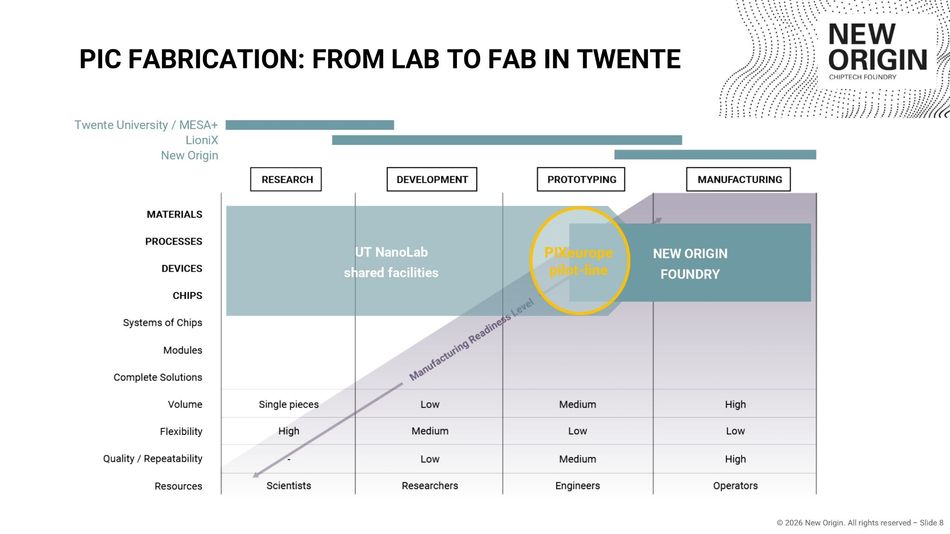
At the same time, many teams face a familiar challenge: moving from successful prototypes to dependable industrial-scale manufacturing.
New Origin was founded to address that gap. Based in the Netherlands, the company is building an independent pure-play SiN foundry focused on providing a seamless transition from R&D to scalable fabrication.
This vision aligns with the goals of the Global Photonics Engineering Contest 2026, which gives participants a pathway from concept and design to fabrication and potential funding. In this ecosystem, New Origin could become a future manufacturing partner for teams ready to scale their innovations.
SiN: A Platform Built for Low-Loss, Scalable Photonics
As integrated photonics expands into markets such as healthcare, consumer electronics, quantum technologies, and AI infrastructure, SiN is gaining momentum as a versatile platform that combines low optical losses, broad wavelength support, and the ability to leverage established manufacturing processes.
For New Origin, SiN serves as the foundation for a manufacturing strategy focused on bridging the gap between research and scalable production.
Peter van Arkel speaks with Twan Korthorst, CEO of New Origin, about the growing role of SiN PICs and the manufacturing infrastructure needed to take them from prototype to volume production. Korthorst brings more than 30 years of experience in semiconductor and photonics technologies. He previously served as the CEO of PhoeniX Software and later led Synopsys’ photonic solutions business following its acquisition.
Peter (PhotonDelta): What makes SiN a strong platform choice for integrated photonics today?
Twan Korthorst (New Origin): SiN is the technology platform of choice for a large variety of applications due to its superior optical performance and broad wavelength spectrum support. Key advantages of SiN include:
Very low propagation losses
Broad wavelength coverage, spanning visible to infrared
Compatibility with standard silicon wafer processing
Ability to scale to 200/300 mm wafers
Relative ease of integrating additional materials and processes
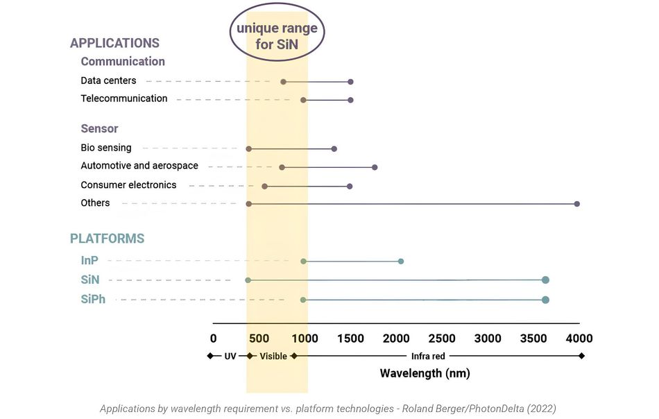
Compared with silicon photonics, SiN offers lower optical losses and broader transparency, which are especially valuable in sensing, healthcare, and quantum applications. Compared with III-V platforms such as indium phosphide, SiN does not provide native light generation, but it excels as a passive waveguide platform and can be combined with active materials when needed. As photonic systems become more complex and move into new markets, these attributes are making SiN an increasingly attractive platform choice.
For participants in the Global Photonics Engineering Contest 2026, it offers a versatile and scalable foundation to develop solutions that can ultimately transition to industrial manufacturing.
Peter (PhotonDelta): Could you tell us something about your products, services, and key initiatives?
Twan Korthorst (New Origin): New Origin is currently in the facility development phase. Backed by significant investment, the company is building a dedicated manufacturing infrastructure focused exclusively on SiN PICs. Its core offering will be pure-play foundry manufacturing for customers developing SiN-based PICs.
The company’s goal is to provide:
Predictable and repeatable manufacturing
Low- to medium-volume, high-mix production
Competitive turnaround times
Support for advanced integration approaches
One of the company’s most notable recent developments is its collaboration with imec. This partnership will transfer imec’s low-pressure chemical vapor deposition (LPCVD) SiN platform to New Origin, helping accelerate industrialization while improving yield and lowering cost.
Suggested reading: Imec on How Datacom and AI Are Accelerating the Maturity of Integrated Photonics: An Interview with Philippe Soussan
The foundry is also being designed to incorporate non-CMOS-compatible materials such as gold and thin-film lithium niobate (TFLN), expanding the range of architectures it can support.
Peter (PhotonDelta): As a pure-play SiN foundry, how does your business model differ from vertically integrated photonics companies, and what advantages does this create for customers?
Twan Korthorst (New Origin): Vertically integrated photonics companies typically develop and manufacture products for their own end markets.
New Origin is taking a different approach.
As a pure-play dedicated PIC foundry, our focus is solely on manufacturing. We don’t compete with our customers. Instead, we will provide the fabrication infrastructure that enables fabless photonics companies to bring products to market.
This model offers several advantages:
Customers retain ownership of their design IP
The foundry can support a broad range of applications
Manufacturing processes can be optimized for repeatability and cost
Companies gain access to industrial-grade production without building their own fab
For strategic applications such as quantum technologies, satellite communications, and healthcare, New Origin sees European manufacturing capacity as an important way to strengthen regional supply chain resilience and long-term technological independence.
Peter (PhotonDelta): What are the key volume applications of SiN? Where do you see the strongest growth?
Twan Korthorst (New Origin): New Origin sees strong growth opportunities across several markets, including:
Augmented and Virtual Reality: Low-loss waveguides and broad wavelength support make SiN well-suited for compact optical engines and display systems.
Biosensing and Healthcare: SiN’s optical properties support highly sensitive detection and imaging systems.
Autonomous Navigation: Applications such as light detection and ranging (LiDAR) and optical sensors benefit from low-loss routing and scalable integration.
Satellite Communications: Photonic integration with SiN can reduce size, weight, and power while improving overall system performance.
Quantum Computing: Quantum systems require highly stable, low-loss optical circuits, making SiN a compelling platform.
Datacom, high-performance computing (HPC), and AI: The rising demand for bandwidth is driving increased adoption of integrated photonics for optical I/O, co-packaged optics, and next-generation interconnects.
Peter (PhotonDelta): One of the key challenges in photonics is scaling production. How is New Origin addressing the transition from research and prototyping to industrial-scale manufacturing?
Twan Korthorst (New Origin): This is the central challenge New Origin was created to solve.
Today, many companies rely on shared research facilities and pilot lines to develop and test SiN-based photonic chips. These environments are invaluable for innovation, but they are not always optimized for production metrics such as yield, cost, and turnaround time.
There is currently no well-established scaling path for SiN photonic chips. New Origin is building a dedicated manufacturing environment focused on industrial execution.
Planned capabilities include:
200 mm wafer processing
Semi-automated operations
Optimized batch sizes for flexible production
Target capacity of 50,000 wafers per year
Process control designed for predictable, repeatable results
This approach is intended to provide the same kind of scalable foundry model that transformed the semiconductor industry.
Peter (PhotonDelta): How can the PhotonDelta Global Photonics Engineering Contest and the broader integrated photonics ecosystem help participants take their ideas from concept to scalable manufacturing
Korthorst (New Origin): For early-stage participants, the broader ecosystem partners can support design and simulation, fabrication through existing foundry resources, testing and validation, and optimization for manufacturability. Once a design is validated and ready to scale, New Origin is positioned to become a part of the manufacturing pathway that helps transition the technology into production.
This staged approach would reduce barriers for startups and research teams by giving them access to specialized expertise and infrastructure throughout the development cycle. In this sense, the contest is more than a showcase. It provides a direct route into an ecosystem designed to turn promising ideas into commercially viable integrated photonic products.
Peter (PhotonDelta): Looking ahead, what is New Origin’s long-term vision?
Korthorst (New Origin): Our ambition is to become a leading global pure-play foundry for photonic chips based on silicon nitride waveguide technology, including non-CMOS compatible materials and processes like, for instance, gold or TFLN. We call this silicon nitride plus (SiN+). The core of our vision is making PICs more accessible by providing manufacturing infrastructure that combines industrial-quality processes, flexible production, support for a wide range of applications, and strong manufacturing capacity within Europe.
We summarize this vision with a simple phrase: “PICs for the masses.”
LEARN MORE ABOUT THE CONTEST AND SUBMIT NOW
Conclusion
SiN has established itself as one of the most versatile and scalable platforms in integrated photonics, but platform advantages alone are not enough. The integrated photonics industry also needs a dependable manufacturing path that can carry designs from research prototypes to commercial production.
That is the opportunity New Origin is pursuing. By building an independent pure-play SiN foundry and embedding it within the European photonics ecosystem, the company aims to provide the industrial foundation needed to scale innovation.
For participants in the Global Photonics Engineering Contest 2026, this is an opportunity to turn innovative ideas into manufacturable photonic products with the support of a world-class ecosystem.