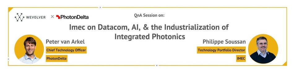
Imec on How Datacom and AI Are Accelerating the Maturity of Integrated Photonics: An Interview with Philippe Soussan
Datacom and AI infrastructure demands are rapidly driving the growth of integrated photonics. Philippe Soussan from imec explains his perspective on the recent developments and how he expects the industry to evolve in the next few years.

07 Apr, 2026. 7 minutes read
imec Leuven (Headquarters), Belgium
Introduction
Integrated photonics has long promised to transform how data moves through modern computing systems. In recent years, the promise has begun translating into industrial reality. The rapid expansion of cloud infrastructure and artificial intelligence places unprecedented demands on bandwidth and power efficiency, all areas where Integrated Photonics offer clear advantages.
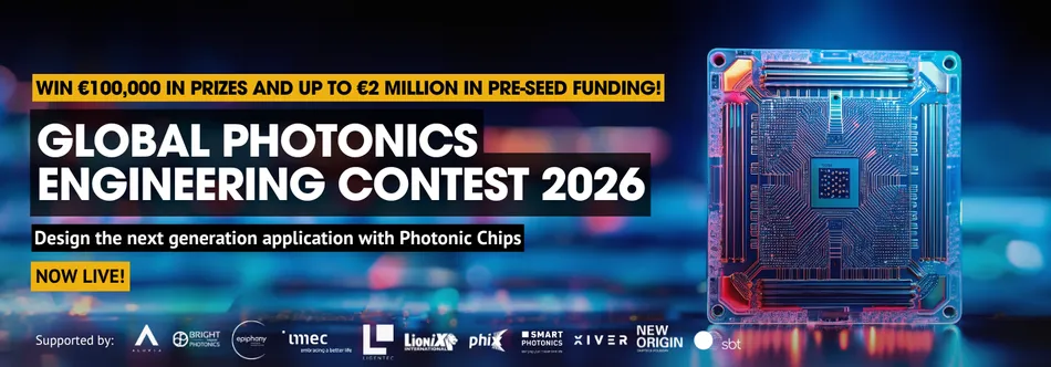
As part of a broader effort to accelerate innovation in photonics, PhotonDelta has launched the Global Photonics Engineering Contest 2026, an initiative to encourage startups, university teams, corporations, research institutions, and the entire photonics community to develop practical solutions for emerging challenges in communication, computing, imaging, wireless, and sensing.
In this discussion, Philippe Soussan talks about how datacom demand has accelerated the industrial maturity of integrated photonics, where key bottlenecks remain, and how the ecosystem is evolving. Philippe is the Technology Portfolio Director for IC-Link silicon solutions, imec and has been with the organization for more than 25 years. He has authored over 100 publications related to photonics.
Peter: Can you tell us about imec and its role in the integrated photonics ecosystem?
Philippe: Imec is a world-leading research and innovation hub in advanced semiconductor technologies. Leveraging its state-of-the-art R&D infrastructure and the expertise of over 6,500 employees, imec drives innovation in semiconductor and system scaling, artificial intelligence (AI), silicon photonics, connectivity, and sensing.
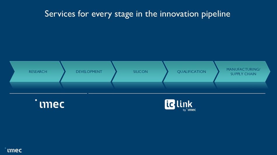
When it comes to integrated photonics, we go from photonics breakthroughs to reliable manufacturing, turning research into commercial impact. In practice, imec’s R&D exploration is developed into platforms that can be commercialized by IC-Link, imec’s division for custom chip manufacturing.
New elements and upgrades from ongoing R&D are continuously incorporated into our photonics PDK to maintain technology offerings. We then provide manufacturing and related services, including supply chain management, for the complete silicon product.
Peter: Imec engages across a wide range of application domains; could you share more details about them?
Philippe: For integrated photonics, AI, particularly datacenter infrastructure, is a hot topic which we are actively involved in – from research to manufacturing. The power, performance, and efficiency that AI demands are crucial. We are working on innovation here that raises the bandwidth density, with 400G per lane and co-packaged optics in our IC-Link portfolio roadmap.
Datacenter infrastructure requirements are driving much of the current momentum in silicon photonics. However, the resulting innovations go far beyond datacom. We see that emerging applications such as quantum and sensing can also benefit, with some additional tweaking based on the specific application. Some examples we are seeing in integrated photonics for industrial and bio-sensing include drug monitoring, glucose and gas monitoring, as well as DNA sequencing, neurosensing, positional sensing, and many more.
Outside photonics and within imec more broadly, our advanced research powers breakthroughs across nearly every sector, including computing, health, automotive, industry, consumer electronics, aerospace, and security.
Peter: Can you share something about the role of the datacom market in accelerating the industrial maturity of integrated photonics?
Philippe: Over the past decade, integrated photonics has experienced a marked increase in production volumes, signaling its transition from early-stage development toward industrial scale.
This growth has come from datacom needs. As more data was moved to the cloud, the need for additional and more efficient hardware in data centers increased to supply data at the edge. As more data went to the cloud, AI was built to process that data with new business models. However, AI needs additional compute power in the data centers, further amplifying the need for additional and more energy-efficient hardware. The co-evolution of data usage and datacenter hardware is what drove the photonics uptake in the last few years and will continue to do so.
Peter: From your perspective, what has fundamentally changed in recent years that makes this moment different from previous waves of integrated photonics innovation? Are there any specific requirements of the datacom market that forced the industry to mature beyond research-driven development?
Philippe: What we see is that energy usage is expected to more than double in the coming 5 years, driven mostly by AI applications.
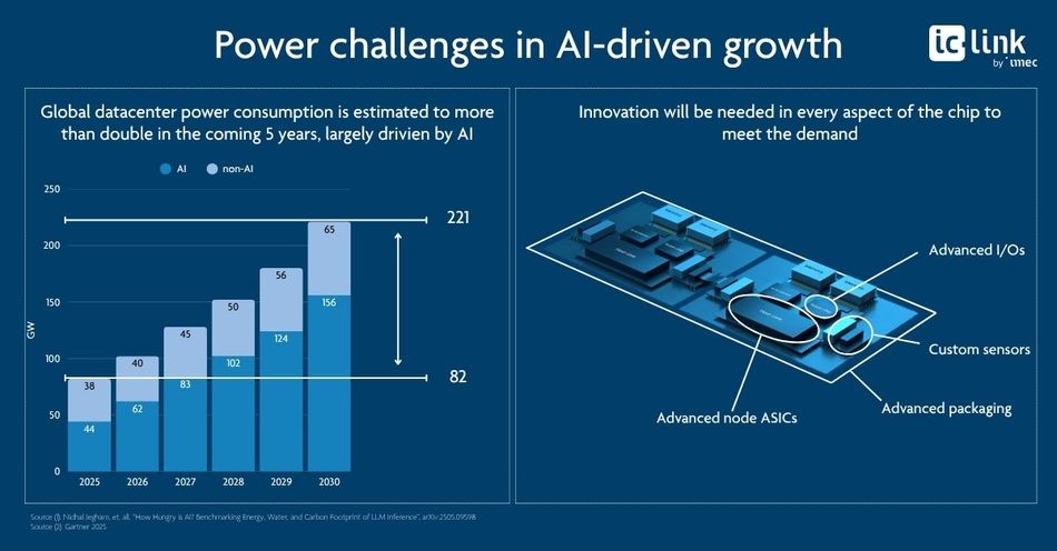
More specifically, this is coming from a societal trend in which people expect data to look for a solution to a question instead of solely figuring out how to access data to find an answer to a problem. This human need for low-friction, instant solutions means that the industry has a clear goal to advance every aspect of the chipset, not only the advanced Input/Outputs (I/Os).
When we do look specifically at the I/Os, we are reaching a point in which the photonics industry has grown to a scale that allows for more standardization. This maturity means that photonics is moving from a captive supplier model to a flexible supply chain that can efficiently carry the volume increases at a competitive cost structure.
This will ultimately enable more efficient hardware, helping to address the power consumption surge expectation.
Peter: You likely see many designs evolve from early-stage research concepts to manufacturable prototypes. In your experience, what distinguishes a compelling laboratory demonstration from a robust, scalable engineering solution ready for industrial deployment?
Philippe: What I see are two differentiators. The first is the underlying technology and how it will develop a design that is really at the forefront of engineering capabilities with the ability to scale up quickly. The second is how the product will fit in the market – whether the market is one that already exists or whether it is bold enough to address a market that is not yet defined.
Peter: Despite recent progress, where does the ecosystem still encounter friction when transitioning from prototype validation to high-volume manufacturing?
Philippe: Even though I mentioned that photonics has made massive leaps in volumes over the past decade, it is still much smaller when looking at CMOS scale. What I mean is that photonics is still in its infancy, relatively speaking. The design methodology still needs to be standardized, but the versatility of the components in the device library makes them more difficult to standardize compared to CMOS, which is very early narrowing technology options. In addition, the number of engineers trained in photonics design remains limited, and the supporting infrastructure is still developing.
Through our IC-Link division, we’ve seen the technological side progress exponentially, making it possible to transition from R&D to high-volume manufacturing. We do this in 2 ways: by being a technology provider to foundries and a technology service provider. We’re making imec PDKs available for designers, supporting these designers and companies with their design, and offering a path to manufacturing. We’re already doing this for integrated photonics on 200 mm and 300 mm wafers, with additional platform features soon coming, including LNO, silicon nitride, and EIC-PIC co-integration for CPO and wide I/O.
Peter: Looking ahead to the coming 5 years, how do you see the integrated photonics landscape evolving? Are there recent collaborations, focus areas, or technology directions that you believe will significantly influence the next phase of industrial maturity?
Philippe: What we see now is that we are moving from vertically integrated models to a more flexible supply chain. This will certainly continue, with companies focusing on their specialty and only their specialty. Ultimately the supply chain will be filled with these specialized parts of the chain and will bring the photonics industry to a higher level.
This is essentially what we saw with the automotive industry. In the early 20th century, auto manufacturers made each part in-house. As the industry grew, they worked with OEM suppliers of different tiers to create their parts, which they would then assemble. I see a similar shift happening in photonics, where companies are increasingly specializing in specific parts of the value chain rather than developing the entire stack in-house.
Where we can play a role is to help ecosystem partners understand this landscape and to further deploy their solutions. Currently imec is actively engaging with different actors of the value chain (tool & EDA vendors, foundries, OSAT, design houses, etc.)
Peter: For teams participating in the Global Photonics Engineering Contest 2026, do you see emerging application areas beyond datacom offering similar opportunities to accelerate industrial maturity, or does datacom remain the primary driver of scalable photonic manufacturing today?
Philippe: The next big wave in photonics is going to be about heterogeneous integration and the adoption of non-silicon materials. We do see datacom remaining as a primary driver for basic building blocks (waveguide, modulator), but that will require the adoption of complex material systems moving further. Emerging applications will benefit, as this is the only viable way to make a large p of the emerging applications operate at the right price point. However, specific differentiation for emerging applications needs to be created to fit markets that still need to grow; for example, in sensing where focus is not on data rate but signal to noise ratio, tunable light source and overall link loss efficiency. Similarly, there is a need to create an ecosystem in the visible range and mid IR, which by the datacenter industry.
At the same time, new initiatives in Europe are helping to build the necessary infrastructure, which could significantly accelerate the development and deployment of these applications toward the end of the decade.
Conclusion
As Philippe’s perspective makes clear, the next stage of progress in photonics will not only depend on scientific breakthroughs but also on engineering solutions that can be manufactured, integrated, and deployed reliably. Bridging that gap between innovation and real-world implementation is now one of the greatest challenges in the field.
This is precisely where new ideas, practical engineering approaches, and interdisciplinary collaboration become critical.
With the Global Photonics Engineering Contest 2026, PhotonDelta is calling on startups, engineers, researchers, and innovators across the photonics ecosystem to develop practical, scalable solutions in key domains such as communication, computing, sensing, imaging, and wireless technologies. Selected participants will gain visibility, access to industry expertise, and the opportunity to accelerate their innovations within the global photonics ecosystem.
Are you working on a photonics solution that could shape the next generation of applications? Learn more and apply here.