Reactive Ion Etching: A Comprehensive Guide
Reactive Ion Etching (RIE) is a powerful and versatile technique that has been widely adopted in various industries including semiconductor manufacturing, microelectromechanical systems (MEMS), and nanotechnology.

11 Apr, 2023. 14 minutes read
Introduction
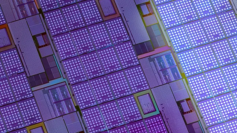
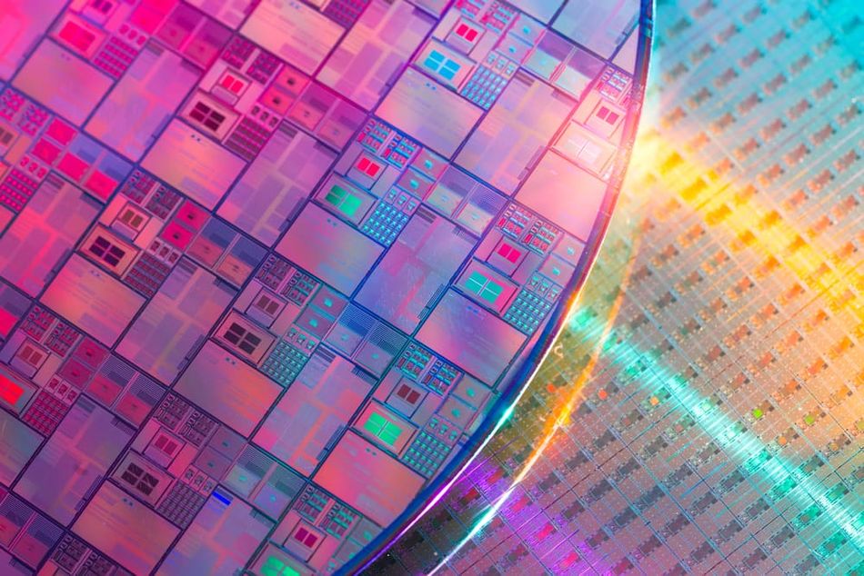
Etching is an important process in microfabrication to chemically remove layers from the wafers. Reactive ion etching (RIE) uses the fourth state of matter- “plasma” to perform etching. The process is categorized into dry etching and generates plasma under a vacuum environment to attack the wafer surface. The ability to create high-resolution, and anisotropic patterns on a variety of materials has made RIE an essential tool for people working all across these industries.
1. The Basics of Reactive Ion Etching
1.1. What is Reactive Ion Etching?
Reactive Ion Etching (RIE) is a dry etching technique widely used in semiconductor manufacturing, MEMS fabrication, microfabrication and nanotechnology to create patterns on the surface of various materials with high resolution and anisotropy. Unlike wet etching methods involving chemical reactions with liquid etchants, RIE uses reactive gases in a plasma state to chemically and physically remove the material from the surface. The use of reactive gases enables RIE to offer better control and precision over the etching process compared to other methods.
1.2. The Etching Process
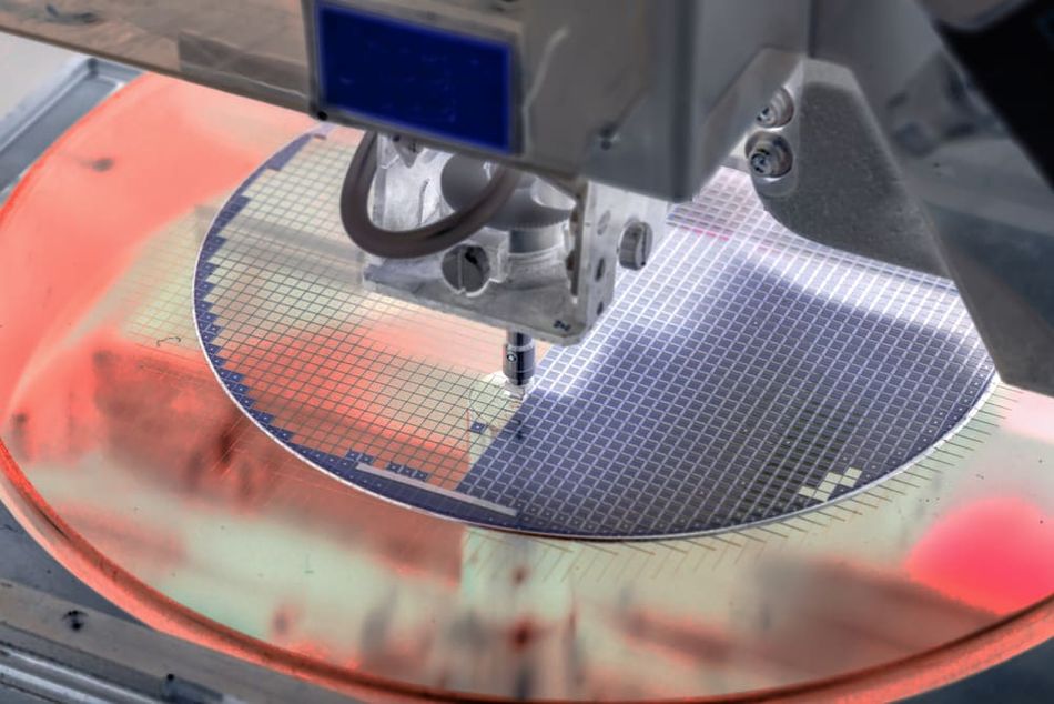
The RIE process starts by placing a substrate, typically a silicon wafer covered with a patterned mask, inside a vacuum chamber. Reactive gases are then introduced into the chamber, and plasma is generated by applying an electric field using electrodes. The plasma consists of a mixture of ions, free electrons, and neutral particles. The electric field accelerates the ions in the plasma towards the substrate, resulting in both chemical reactions and physical sputtering at the surface. The combination of these two mechanisms removes the material selectively to create the desired pattern.
1.3. Advantages of Reactive Ion Etching
One of the most significant benefits of RIE over other chemical etching methods is its ability to achieve high etch rates and anisotropy. The ion bombardment in RIE allows better control of the etching direction compared to isotropic plasma etching. The direction control results in sharp and well-defined features with minimal undercutting. Additionally, RIE is a versatile technique that can be used on materials including metals, semiconductors, and insulators in several applications. Furthermore, RIE etching is a dry etching method that avoids drawbacks associated with wet etching like contamination and the handling of hazardous chemicals.
2. Key Components of a Reactive Ion Etching System
2.1. Vacuum Chamber
The vacuum chamber is the central component of a reactive ion etching system that provides a controlled environment for the etching process to occur. The chamber is designed to maintain a low-pressure environment, which is crucial for generating stable plasma and generating precise etching results. The walls of the chamber are usually made of corrosion-resistant materials like stainless steel or aluminium to withstand the reactive gases and byproducts generated during the process. The vacuum is maintained by an exhaust system that continuously removes the gases and etching byproducts from the chamber, which will be discussed in detail in section 2.4.
2.2. Gas Delivery System
The gas delivery system is responsible for introducing and controlling the reactive gases used in the etching process. This system typically consists of gas cylinders, mass flow controllers, and a manifold that connects them to the vacuum chamber. The mass flow controllers precisely regulate the flow rate of the gases, ensuring a consistent and reproducible etching process. The choice of reactive gases is critical to the RIE process, as it determines the etch rate, selectivity, and anisotropy. Commonly used reactive gases include chlorine (Cl2), fluorine (F2), and sulfur hexafluoride (SF6). The reactive gases are chosen based on the etcher material used and the desired etching characteristics.
2.3. Power Supply and Electrodes
The power supply and electrodes play a crucial role in generating and controlling plasma processing in a reactive ion etching system. The power supply is connected to the electrodes, which are usually placed inside the vacuum chamber. When a high-frequency voltage is applied to the electrodes, it ionizes the reactive gases to create a plasma. The electric field generated by the electrodes accelerates the ions towards the substrate, causing both chemical and physical etching. The power supply typically operates in the radio frequency (RF) range, with common frequencies between 13.56 MHz and 27.12 MHz. The choice of power and bias voltage directly impacts the ion energy and etching characteristics, which will be discussed further in section 4.3.
2.4. Exhaust System
The exhaust system is a vital component of a reactive ion etching system responsible for maintaining the vacuum environment within the chamber and eliminating the etching byproducts. The system usually consists of a vacuum pump like a turbomolecular pump or a cryopump connected to the chamber through a series of valves and piping. The exhaust system must be designed to handle the specific reactive gases and byproducts generated during the RIE process, ensuring that they are safely and efficiently removed from the chamber. This not only maintains the vacuum conditions required for the process but also prevents contamination and potential damage to the etched structures.
3. Reactive Ion Etching Gases and Materials
3.1. Commonly Used Reactive Gases
The choice of reactive gases plays a crucial role in the RIE process because it directly affects the etching characteristics including etch rate, selectivity, and anisotropy. Some of the most commonly used reactive gases in RIE are:
Chlorine (Cl2): Chlorine is frequently used for etching silicon, metals, and compound semiconductors. It is highly reactive and can achieve high etch rates, but it can also be corrosive to certain materials and chamber components.
Fluorine (F2): Fluorine is often used for etching oxides like silicon dioxide (Sio 2), silicon nitride, and other dielectric materials. It is highly selective to enable precise control over the etching process. However, Flourine gas molecules can be highly reactive with certain materials that may require additional precautions during RIE.
Sulfur Hexafluoride (SF6): SF6 is commonly employed for etching silicon, glass, and other insulating materials. It has a lower etch rate compared to chlorine and fluorine but offers good selectivity and anisotropy.
Boron Trichloride (BCl3): BCl3 is often used in conjunction with chlorine to etch compound semiconductors, such as gallium arsenide (GaAs), gallium nitride (GaN) and indium phosphide (InP). The combination of BCl3 and Cl2 allows for precise control over the etching process and improved selectivity.
The choice of reactive gas depends on the material being etched and the desired etching characteristics. In some cases, a mixture of gases may be used to achieve the optimal balance between etch rate, selectivity, and anisotropy.
3.2. Material Compatibility
Understanding the compatibility between different materials and reactive gases is essential for successful RIE. Different materials exhibit varying etching characteristics depending on the reactive gases used, making it crucial to select the appropriate gas for a specific material. For example, chlorine-based gases are effective for etching silicon and compound semiconductors, while fluorine-based gases are more suitable for etching dielectric materials, oxides like silicon dioxide, and silicon nitride (photoresist).
Moreover, the choice of reactive gas can also impact the selectivity of the etching process, which refers to the ability to etch one material while leaving another relatively unaffected. This is particularly important when etching multilayer structures or using a masking material during the RIE process. By understanding the compatibility between materials and reactive gases, one can optimize the etching process for the desired outcome, ensuring high-quality results and minimal damage to the substrate or masking layers.
4. Key Parameters in Reactive Ion Etching
4.1. Pressure
The pressure within the vacuum chamber is a critical parameter in the RIE process that directly impacts the density of the plasma. It is also responsible for the mean free path of the particles within the chamber. Lower pressures typically result in a higher-density plasma, leading to increased etch rate and anisotropy. However, low pressure makes the mean free path of the particles long enough to decrease the etch rate and uniformity. Conversely, higher pressures can lead to a lower plasma density and reduced anisotropy because the ions experience more collisions and have a shorter mean free path. Therefore, finding the optimal pressure for a specific RIE process is crucial to achieving the desired etching characteristics.
4.2. Gas Flow Rate
The gas flow rate is another important parameter in RIE that determines the concentration of reactive species in the chamber and affects the etching process's stability and reproducibility. Balancing the gas flow rate is essential to achieve the desired etching performance while maintaining process stability and uniformity. A higher gas flow rate can increase the etch rate by introducing more reactive species into the plasma. However, an extremely high gas flow rate may also lead to decreased uniformity and selectivity. A lower gas flow rate can result in a more stable and uniform etching process, but at the cost of reduced etch rates.
4.3. Power and Bias Voltage
The power and bias voltage applied to the electrodes in the RIE system significantly influence the plasma density and the energy of the ions accelerated towards the substrate. A higher power and bias voltage result in a higher plasma density and increased ion energy, leading to faster etching rates and improved anisotropy. However, higher ion energies can also cause damage to the substrate or etched structures in delicate or small-feature applications.
On the other hand, lower power and bias voltage settings can reduce the risk of damage to the substrate but may also result in lower etching rates and anisotropy. Consequently, optimizing the power and bias voltage for a specific RIE process is crucial to ensure the desired etching performance while minimizing the risk of damage to the substrate or etched features.
4.4. Temperature
Temperature is another key parameter in the RIE process to affect both the chemical and physical aspects of the etching. Higher substrate temperatures can enhance the chemical reactions between the reactive species and the substrate material, leading to increased etching rates. However, higher temperatures can also cause increased diffusion of the reactive species that may potentially reduce the selectivity and anisotropy of the etching process.
In contrast, lower temperatures can improve the selectivity and anisotropy of the RIE process, but reduce the etching rates. Additionally, low temperatures can cause the condensation of reactive gases or byproducts on the chamber walls, which may lead to contamination issues. Therefore, careful management of the temperature within the RIE system is vital to achieving the desired etching performance and avoiding potential problems.
5. Reactive Ion Etching Techniques and Configurations
5.1. Parallel Plate RIE
Parallel Plate RIE is the most basic and widely used configuration in reactive ion etching systems. Two parallel electrodes are placed inside the vacuum chamber, with one electrode connected to the RF power supply and the other grounded. The substrate is typically placed on the grounded electrode when the reactive gases are introduced into the chamber. Upon application of RF power, plasma is generated between the electrodes. The ions accelerate towards the substrate, causing both chemical and physical etching. This configuration is simple, cost-effective and ideal for many applications in semiconductor manufacturing and MEMS fabrication.
5.2. Inductively Coupled Plasma (ICP) RIE
Inductively Coupled Plasma (ICP) RIE is an advanced RIE technique that offers improved plasma density and process control compared to parallel plate RIE. In this configuration, an RF coil wrapped around the vacuum chamber generates the plasma instead of parallel electrodes. When the RF power is applied, an oscillating magnetic field is generated that creates a high-density plasma inside the chamber. A separate RF bias voltage is applied to the substrate holder for controlling the ion energy and directionality. Compared to parallel plate RIE, this configuration enables higher plasma densities and lower operating pressures that in faster etching rates and improved anisotropic etch.
5.3. Deep Reactive Ion Etching (DRIE)
Deep Reactive Ion Etching (DRIE) is a specialized RIE technique designed for etching high-aspect-ratio features in silicon substrates, such as trenches or through-silicon vias (TSVs) used in MEMS and 3D ICs. Also known as the Bosch process, DRIE utilizes a cyclic process alternating between an etching step using reactive gases like SF6, and a passivation step using gases like C4F8. During the etching step, the reactive gas removes the silicon material, while the passivation step deposits a protective polymer film on the sidewalls of the etched features. This cyclic process results in highly anisotropic and deep etching profiles, with aspect ratios of up to 100:1 or more.
5.4. Reactive Ion Beam Etching (RIBE)
Reactive Ion Beam Etching (RIBE) is another variant of the RIE process that uses an ion beam source instead of electrodes or coils to generate the plasma. In RIBE, the reactive gases are ionized in an external ion source and then accelerated towards the substrate as a focused ion beam. This configuration allows for precise control over the ion energy and directionality, leading to highly anisotropic and selective etching. RIBE systems tend to be more complex and expensive than traditional RIE systems, making them less common in the industry.
Each of these RIE techniques and configurations has its advantages and drawbacks. One can choose the correct method depending on factors such as the desired etching characteristics, the material being etched, and the specific application requirements. By understanding the working principles and technical depth of each technique, the RIE process can be optimized for particular needs.
6. Challenges and Solutions in Reactive Ion Etching
6.1. Profile Control
One of the main challenges in RIE is achieving precise profile control, which refers to the ability to maintain the desired shape and dimensions of the etched features. Factors that can influence profile control include ion directionality, plasma uniformity, and the choice of reactive gases. To improve profile control, one can optimize the RIE process parameters including pressure, power, and gas flow rate. Another way to improve profile control is by employing advanced RIE techniques like Inductively Coupled Plasma (ICP) RIE or Deep Reactive Ion Etching (DRIE) that offer better ion directionality and anisotropy.
6.2. Etch Rate Uniformity
Achieving uniform etch rates across the entire substrate surface is another challenge in RIE. It is because on-uniform etching can lead to variations in feature dimensions and degraded device performance. Factors that can affect etch rate uniformity include chamber design, gas flow distribution, and RF power distribution. Optimization of chamber geometry, gas injection system, and RF power delivery improves etch rate uniformity. Furthermore, employing real-time process monitoring and control techniques enables maintaining consistent etching conditions throughout the process for etch rate uniformity.
6.3. Selectivity
Selectivity is a critical parameter in RIE to determine the ability to etch one material while leaving another relatively unaffected. Achieving high selectivity can be challenging, especially dealing with multilayer structures or when using masking materials with similar etching properties to the target material. To improve selectivity, one can carefully select the reactive gases and process conditions, or employ techniques like Atomic Layer Etching (ALE) for having precise control over the etching process at the atomic scale.
6.4. Substrate Damage
Substrate damage is a major concern in RIE, as high-energy ions and reactive species can cause physical and chemical damage to the substrate or etched structures. Factors that can contribute to substrate damage include ion energy, reactive gas chemistry, and etching byproducts. To minimize substrate damage, one can optimize the process parameters like power and bias voltage. Employing techniques like low-damage RIE utilizes lower ion energies and less aggressive reactive gases to reduce the risk of damage.
6.5. Contamination and Particle Generation
Contamination and particle generation are critical issues in RIE that may lead to defects in the etched features and reduced device yield. Sources of contamination include residual gases, chamber materials, and etching byproducts. To mitigate contamination and particle generation, one can implement rigorous process control and chamber cleaning procedures, and use high-purity reactive gases and materials. Using advanced plasma diagnostics and real-time monitoring techniques to detect and address contamination issues during the RIE process.
Limitations and challenges of reactive ion etching can be overcome by understanding the working principles. The RIE method optimises for different applications by implementing relevant solutions that may result in high-quality outcomes and improved device performance.
7. Reactive Ion Etching Applications
7.1. Semiconductor Manufacturing
Reactive ion etching is widely used in semiconductor manufacturing for various processes, such as the fabrication of integrated circuits (ICs), microelectromechanical systems (MEMS), and photovoltaics. RIE is employed to create intricate patterns in thin films, define the shape and size of transistors, and etch high-aspect-ratio features like vias and trenches. The ability to achieve high selectivity, anisotropy, and precise profile control makes RIE an indispensable tool in semiconductor manufacturing.
7.2. MEMS Fabrication
Microelectromechanical systems (MEMS) are miniaturized devices that combine mechanical and electrical components including sensors, actuators, and microfluidic structures. RIE plays a crucial role in MEMS fabrication by enabling the precise etching of intricate structures and patterns in various materials like silicon, polymers, and metals. Deep Reactive Ion Etching (DRIE) is particularly useful in MEMS fabrication for creating high-aspect-ratio features, such as deep trenches, channels, and through-silicon vias (TSVs).
7.3. Nanotechnology and Nanofabrication
Nanotechnology and nanofabrication involve the design and manipulation of materials and structures at the nanometer scale to serve applications in electronics, photonics, biotechnology, and many more industries. RIE is an essential tool in nanofabrication that allows precise patterning and etching of nanoscale structures and devices. Techniques such as Atomic Layer Etching (ALE) can provide atomic-scale control over the etching process, and enable the fabrication of advanced nanodevices with unprecedented precision and accuracy.
7.4. Photonics and Optoelectronics
Photonics and optoelectronics are fields that focus on the generation, manipulation, and detection of light. RIE is a crucial process in the fabrication of photonic and optoelectronic devices, such as waveguides, lasers, photodetectors, and modulators. The ability to achieve high anisotropy and profile control enables the creation of complex and intricate structures in a variety of materials, including semiconductors, dielectrics, and metals.
7.5. Surface Modification and Functionalization
Reactive ion etching is not only used for the removal of material but also for modifying and functionalizing surfaces. RIE can be employed to create micro- and nano-scale patterns, textures, and features on various surfaces. It can alter the properties and characteristics including wettability, adhesion, and biocompatibility. This capability has applications in areas like biomaterials, surface coatings, and advanced materials research.
By understanding the technical depth of reactive ion etching, one can appreciate its versatility and wide range of applications across various industries and fields. This powerful technology enables the creation of sophisticated devices and structures with unparalleled precision and control to pave the way for advancements in numerous domains.
8. Future Trends and Advancements in Reactive Ion Etching
8.1. Atomic Layer Etching (ALE)
Atomic Layer Etching (ALE) is an emerging RIE technique that provides atomic-scale control over the etching process. ALE is a cyclic process that alternates between the exposure of the substrate to reactive gases and the removal of the modified surface layer, enabling precise control of the etching depth and feature dimensions. This technique holds great promise for future applications in nanofabrication, semiconductor manufacturing, and advanced materials research. It is because ALE can achieve even higher precision, selectivity, and uniformity compared to traditional RIE methods.
8.2. Plasma Diagnostics and Real-time Process Control
Advancements in plasma diagnostics and real-time process control techniques are expected to play a significant role in the future of RIE. By employing advanced sensors in monitoring, and feedback control systems, RIE process parameters can be optimised dynamically. Such parameters ensure consistent and uniform etching results across the substrate. This capability will be particularly beneficial for large-scale complex production, and multi-step fabrication processes where even minor variations in etching conditions can lead to significant yield losses and reduced device performance.
8.3. Environmentally Friendly and Sustainable Etching Processes
As the demand for environmentally friendly and sustainable manufacturing processes grows, the development of new RIE techniques increases. The chemistries that minimize the use of hazardous materials and reduce waste generation will become increasingly important. This could involve the development of novel reactive gas mixtures, alternative plasma sources, or low-damage RIE processes that enable efficient etching with less environmental impact. The adoption of such green etching processes will be crucial in ensuring the long-term sustainability of the semiconductor and electronics industries.
8.4. Integration with Other Nanofabrication Techniques
The need of integrating RIE with other advanced nanofabrication techniques, such as electron-beam lithography, focused ion beam milling, or nanoimprint lithography is increasing. The implementation of such techniques is expected to enable the fabrication of even more complex and sophisticated devices and structures. By combining the strengths of these various techniques, researchers and engineers can push the boundaries of what is possible in terms of feature size, complexity, and functionality. Such technology will pave the way for new discoveries and applications in electronics, photonics, biotechnology, and beyond.
8.5. Machine Learning and Artificial Intelligence in RIE
The application of machine learning and artificial intelligence (AI) in the optimization and control of RIE processes is an exciting area of future research. By harnessing the power of AI algorithms and data-driven modelling, it may be possible to predict and optimize the RIE process parameters more effectively. Deploying ML and AI would result in improved etching performance, reduced trial-and-error experimentation, significant cost savings, higher device yields, and faster innovation in the semiconductor and electronics industries.
By understanding the working principles of reactive ion etching, we can anticipate and contribute to future trends and advancements in this critical technology. As the demand for smaller, faster, and more energy-efficient devices continues to grow, innovations in RIE will play a pivotal role in enabling the next generation of electronic and photonic devices.
Conclusion
Reactive ion etching (RIE) is a versatile and powerful technology that has revolutionized the semiconductor, electronics, and photonics industries. By understanding the working principles and technical depth of RIE, we can appreciate its widespread applications and the crucial role it plays in the fabrication of complex devices and structures. The ability to achieve high anisotropy, selectivity, and profile control has made RIE an indispensable tool for the precise etching and patterning of various materials.
However, challenges in RIE like profile control, etch rate uniformity, selectivity, substrate damage, and contamination need to be addressed. With advancements in plasma diagnostics, real-time process control, and the development of novel techniques like Atomic Layer Etching (ALE), the future of RIE looks promising.
The integration of RIE with other advanced nanofabrication techniques and the application of machine learning and artificial intelligence in RIE optimization and control is expected to further push the boundaries of what is possible in terms of feature size, complexity, and functionality.
In conclusion, reactive ion etching is a critical technology that has shaped the landscape of modern electronics and will continue to drive innovations and advancements in various industries and fields. By understanding the working principles and technical depth of RIE, researchers, engineers, and manufacturers can harness their full potential to create sophisticated devices and structures that will define the future of electronics, photonics, and many more industries.
References
[1] Lieberman, M. A., & Lichtenberg, A. J. (2005). Principles of Plasma Discharges and Materials Processing (2nd ed.). Hoboken, NJ: John Wiley & Sons, Inc.: https://www.wiley.com/en-us/Principles+of+Plasma+Discharges+and+Materials+Processing%2C+2nd+Edition-p-9780471720010
[2] Jansen, H., Gardeniers, H., de Boer, M., Elwenspoek, M., & Fluitman, J. (1996). A survey on the reactive ion etching of silicon in microtechnology. Journal of Micromechanics and Microengineering, 6(1), 14-28. https://doi.org/10.1088/0960-1317/6/1/003
[3] Laermer, F., & Schilp, A. (2003). Method of anisotropically etching silicon. US Patent No. 6,528,350. U.S. Patent and Trademark Office, Washington, DC. https://patents.google.com/patent/US5501893A/en
[4] Kanarik, K. J., Lill, T., Hudson, E. A., Sriraman, S., Tan, S., & Marks, J. (2018). Overview of atomic layer etching in the semiconductor industry. Journal of Vacuum Science & Technology A: Vacuum, Surfaces, and Films, 36(2), 020801. https://doi.org/10.1116/1.5011790
Recommendations: https://www.wevolver.com/article/castellated-holes-the-ultimate-guide-to-their-advantages-and-applications
https://www.wevolver.com/article/deoxidizing-aluminum-as-a-pretreatment
in this article
1. Introduction1. The Basics of Reactive Ion Etching2. Key Components of a Reactive Ion Etching System3. Reactive Ion Etching Gases and Materials4. Key Parameters in Reactive Ion Etching5. Reactive Ion Etching Techniques and Configurations6. Challenges and Solutions in Reactive Ion Etching7. Reactive Ion Etching Applications8. Future Trends and Advancements in Reactive Ion Etching10. Conclusion11. References