Nexperia Wide Bandgap Selection Guide
Nexperia links device-level advantages to application requirements, helping designers choose the best Wide bandgap (WBG) solution for their design.

27 May, 2026. 15 minutes read

Introduction
The meteoric rise of electrification, automation, and digital infrastructure is placing notable strain on existing power systems. Whether it’s the electric-vehicle trend toward 800 V architectures or renewable-energy systems demanding higher efficiency under partial-load operation, power designers need to meet new and challenging design constraints every day. Regardless of the application, efficiency, thermal management, and system size are now tightly interconnected considerations for the system designer.
For decades, most designers have turned to silicon as their primary solution for power system design. However, as power requirements are becoming more complex, this narrative is now changing. Wide bandgap (WBG) semiconductors—specifically silicon carbide (SiC) and gallium nitride (GaN)—now unlock higher electric field and temperature capabilities, faster switching speeds, and reduced switching losses for power systems.
Despite the benefits of WBG, designers face challenges deciding which technologies are best suited for a given application. Selecting the right device requires a deep, expert understanding of how device physics translates into real system behavior.
Nexperia is helping designers navigate these challenges with a broad portfolio of devices that spans silicon IGBTs, SiC Schottky diodes, SiC MOSFETs up to 1200 V, and GaN FETs in cascode and enhancement-mode configurations. Nexperia’s devices offer lower RDS(on) temperature stability, narrow threshold voltage tolerance, great gate charge characteristics, and advanced thermal packaging options.
In this guide, we’ll help readers connect device-level advantages directly to application requirements, so that designers can select the optimal WBG solution for their design.
Application-First Approach to Device Selection
Selecting SiC or GaN should always begin with a clear understanding of the application environment and the demands it places on the system’s operating envelope. Some of the important criteria include
Blocking voltage: Different applications must withstand different voltages. For example, a system operating at 400V nominal bus voltage can be addressed using 650V GaN devices or 650/750V SiC MOSFETs, and sometimes, according to customer qualification requirements and application topology, especially in the Automotive field, the 750V SiC devices. When the system is at 800V nominal bus voltage for a single-level topology, 1200V SiC MOSFETs have to be selected. New Multilevel topologies, even at 800V battery bus voltage, can use stacked 650V/750V switches. For lower switching frequency and high-power applications, the IGBT can be considered a possible solution, even with the same voltage-class selection.
Switching frequency: As switching frequency increases, switching losses become proportionally more important than conduction losses. GaN devices excel at high switching frequencies above 200 kHz due to low QG and QOSS, while SiC devices provide an optimal compromise at moderate switching frequencies (40 to 150kHz) with superior high-voltage capability.
Load profile: Designers of systems at high load need to prioritize conduction loss and thermal stability. High-load systems can benefit from SiC FETs with low RDS(on drift over temperature and predictable conduction loss. In contrast, systems that spend significant time at partial load may benefit from GaN devices with superior dynamic performance due to low gate charge.
Hard versus soft switching: Hard-switching versus soft-switching topologies further complicate device selection. In hard-switching totem-pole PFC, reverse recovery and output charge dominate efficiency. In resonant LLC converters, the behavior of the output capacitance influences the zero-voltage switching boundaries. Knowing the topology will inform your choice of switching device and k parameters for an efficient selection.
Thermal constraints: The expected power dissipation and ambient conditions will inform much of your system design. Knowing your thermal tolerance and available cooling methods will help you choose the right power device and the correct package for your environment. Usually, higher power applications with specific cooling systems prefer top side cooling packages for better management of the junction temperature increase at heavy load.
Power density and size constraints: When minimizing volume, weight, and passive component size is important. Device selection must prioritize switching speed, loss reduction, and packaging efficiency.
With these criteria defined, an application-first approach to device selection becomes clear.
Application #1: EV Charging (On-Board and Off-Board)
EV charging systems operate primarily in the 650-1200 V voltage class and are one of the most demanding environments for wide bandgap devices. Today’s automotive architectures are commonly based on totem-pole PFC stages at the front end, followed by LLC or other isolated DC-DC converters. In some cases, designs will include inverter stages for bidirectional energy transfer for vehicle-to-load or vehicle-to-grid operation. These systems must deliver high efficiency under sustained load while maintaining strict thermal and reliability margins. Faced with extended charging durations and elevated operating temperatures, designers must carefully balance voltage headroom, switching performance, and long-term thermal stability when selecting devices.
Selection Guidance
In 800 V platforms, designers need 1200 V devices to ensure sufficient voltage margin. SiC MOSFETs are therefore the preferred solution in primary switching stages of both totem-pole PFC and isolated DC-DC converters. Their stable RDS(on) over temperature reduces conduction losses at elevated junction temperatures, which is non-negotiable during long charging cycles. SiC’s narrow threshold voltage tolerance also supports reliable paralleling in higher-current systems.
For lower-voltage chargers operating at 400V, GaN FETs can be highly effective in the PFC stage. Their negligible reverse recovery and low QOSS reduce switching losses in soft-switching topologies such as resonant DC/DC converters, while Qgd and negligible Qrr are k parameters for hard switching applications, such as bridgeless totem-pole PFC for the fast leg selection. However, as voltage requirements approach 800 V, 1200V SiC provides greater robustness and voltage headroom in a single-level topology.
SiC Schottky diodes based on merged PiN Schottky technology are widely used in boost and rectification stages due to their minimal reverse recovery losses and high current capability.
Performance Comparison
Silicon: Silicon devices struggle to achieve high efficiency in totem-pole PFC applications because reverse-recovery losses increase switching energy and limit achievable frequency, but they can be used in the slow leg to freewheel current.
GaN: GaN eliminates reverse-recovery charge, making it highly efficient for sub-650 V PFC designs and multi-level topologies (e.g., T-type or Vienna PFC, especially 650 V BDS solutions). Fast switching capability assures low switching losses and higher efficiency in hard switching at higher switching frequencies.
SiC: For 800 V systems, SiC provides the strongest balance of voltage capability, switching speed, and thermal stability. Reduced RDS(on) drift over temperature improves real-world efficiency in high-power applications compared to devices with higher temperature coefficients.
Package Guidance
Package choice directly affects thermal and electrical performance. TO-247-4 packages suit high-power off-board chargers where large heatsinks are acceptable. D2PAK-7 supports automotive-qualified surface-mount designs.
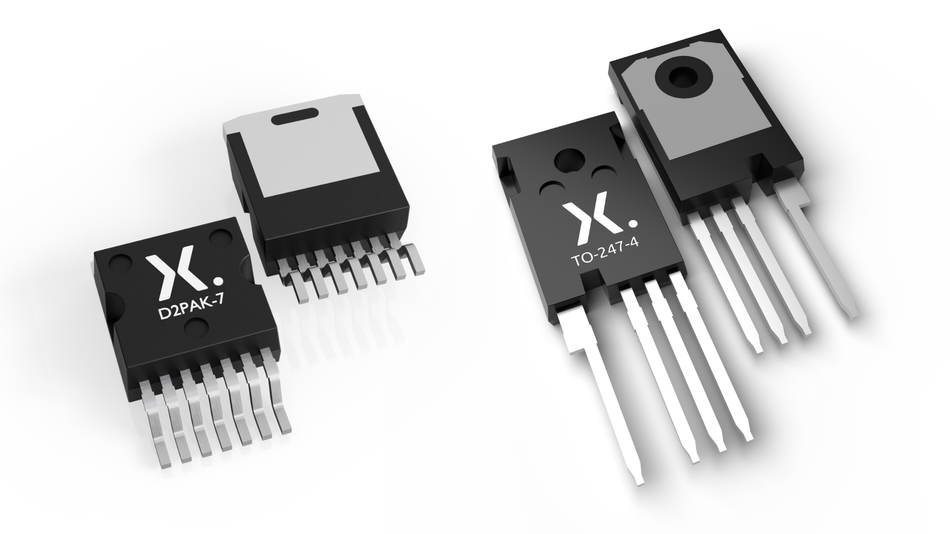
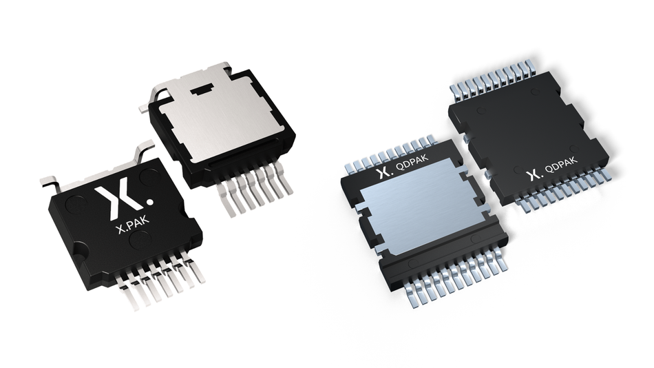
Top-side cooled packages such as X.PAK and QDPAK can unlock compact onboard charger layouts by improving heat extraction and reducing PCB thermal stress. Their low inductance also supports stable high dv/dt switching, reducing turn-on losses as well.
Application #2: Solar Inverters and Energy Storage Systems
Solar inverters and energy storage systems typically operate in the 600 to 1200 V voltage class and are designed for long operational lifetimes under highly variable load conditions. Common topologies include half-bridge and full-bridge inverter stages for DC-AC conversion, LLC converters in isolated battery systems, and MPPT boost stages that optimize energy harvest from photovoltaic arrays. These systems must maintain high efficiency between wide load ranges, particularly at partial load when solar generation fluctuates. As a result, engineers need to balance voltage margin, switching performance, and thermal stability to guarantee reliable grid-connected operation over decades of service. New topologies like HERIC inverters or Matrix one are emerging topologies in which BDS 650V GaN switches can boost efficiency and increase power density per unit area.
Selection Guidance
For string inverters, central inverters, and battery energy storage converters operating at 800 to 1000 V DC bus voltages, 1200 V SiC MOSFETs are the preferred primary switching devices. Voltage margin is required for grid-connected systems to withstand transient overvoltages and fault events. SiC MOSFETs provide the required blocking capability while maintaining low switching energy and stable conduction performance.
In partial-load operation, switching losses often dominate overall efficiency. SiC MOSFETs offer low Eon and Eoff values combined with predictable RDS(on) temperature behavior. Reduced RDS(on) drift over temperature improves real-world efficiency during hot daytime operation when junction temperatures rise.
SiC Schottky diodes using merged PiN Schottky technology are widely used in MPPT boost stages and freewheeling functions. Their negligible reverse recovery charge minimizes switching stress and improves efficiency in high-frequency boost converters.
GaN FETs may be suitable in microinverters or lower-voltage residential systems below 650 V, particularly where high switching frequency and compact design are prioritized. However, in larger grid-tied and storage systems, SiC is the dominant technology due to voltage capability and robustness.
Performance Comparison
Silicon: Silicon devices face efficiency limitations in inverter topologies due to higher switching losses and significant reverse recovery charge. These losses become more pronounced at elevated switching frequencies required for higher power density. On top of that, without specific features for addressing fast diode recovery, high-voltage Si MOSFETs can fail at light load conditions, where usually the resonant converters can lose the ZVS /ZCS working conditions due to the dynamic dV/dt issue
GaN: GaN devices offer excellent switching performance in sub-650 V systems, with low QG/QGD and negligible reverse recovery. However, voltage margin constraints limit their use in higher-voltage grid applications.
SiC: SiC provides the optimal balance in 800 and 1000 V solar systems. It combines high voltage capability with low switching losses and strong thermal resilience. Stable RDS(on) behavior across temperature reduces conduction losses during peak solar generation when thermal stress is highest.
Package Guidance
Package selection depends on system power level and cooling strategy. TO-247-4 packages are suitable for high-power industrial and utility-scale inverters because they offer low thermal resistance to an external heatsink and high creepage and clearance distances. Meanwhile, D2PAK-7 is better suited for compact surface-mount designs in residential systems.
Top-side-cooled packages such as X.PAK and QDPAK combine the assembly advantages of SMD technology with direct heat extraction through the package top, allowing designers to route heat away from the PCB, reduce loop inductance, and achieve higher power density in compact designs.
Application #3: Industrial Motor Drives (1-30 kW)
Industrial motor drives in the 600 to 1200 V voltage class are widely used in factory automation, pumps, compressors, robotics, and HVAC systems. These systems typically employ three-phase inverter stages to control AC motors and, in higher-performance or regenerative installations, active front-end (AFE) topologies to deliver bidirectional power flow and improved power factor.
Operating conditions can vary significantly between high-torque, low-speed operation and high-speed switching regimes, requiring devices that balance conduction efficiency and thermal robustness. In this voltage range, power device selection must account for sustained load conditions, regenerative events, and demanding industrial reliability expectations.
Selection Guidance
For motor drives operating with a DC bus voltage above 600 V and approximately 5 kW or more, SiC MOSFETs are generally the preferred device. Their high-voltage capability provides the necessary margin for transient events such as regenerative braking or sudden load changes. In high-torque operation, conduction losses dominate. SiC’s stable RDS(on) performance over temperature helps guarantee predictable current handling under increased junction temperatures.
The positive temperature coefficient of SiC FET RDS(on) also supports natural current balancing in parallel configurations, which can be important in higher-power drive modules. And, with narrow threshold voltage tolerance, SiC offers even greater switching symmetry and can reduce dynamic imbalances in multi-device inverter legs. Moreover, due to a proper Crss/Ciss ratio of the latest SiC MOSFETs technologies, in Half bridge topology, the basic leg of each inverter, SiC MOSFETs are less sensitive to Miller effect and Parasitic Turn On (PTO) due to high dV/dt.
For lower-power servo drives below roughly 1.5 kW, systems use very high PWM frequency to improve control resolution and reduce acoustic noise. In these cases, GaN FETs can be advantageous. Low switching losses and low gate charge enable higher switching frequency without an excessive efficiency penalty, even in 48V battery-bus systems typically used for humanoid robots and battery-fed power and garden tools. However, in higher-voltage, higher-current industrial systems, SiC remains the more robust solution, especially for high-power systems.
Performance Comparison
Silicon: Silicon IGBTs are cost-effective in some lower-frequency motor drives but suffer from higher switching losses and slower transitions. As switching frequency increases to improve motor control precision, these losses become more significant.
GaN: GaN devices offer excellent switching performance in lower-voltage drives, offering higher PWM frequencies ( around 100kHz) and reduced filter size. However, voltage and ruggedness constraints limit their use in larger industrial drives.
SiC: SiC MOSFETs provide the strongest overall trade-off for medium- to high-power drives. They combine fast switching performance with strong conduction efficiency and thermal resilience. Reduced RDS(on) drift over temperature improves efficiency during sustained high-load operation, which is common in industrial environments.
Package Guidance
For >5 kW, 600 to 1200 V three-phase inverters, TO-247-4 are the most suitable choice. The through-hole format supports direct mounting to external heatsinks, provides generous creepage and clearance for high-voltage DC buses, and handles high RMS phase current with strong mechanical stability. The 4-lead configuration also reduces common-source inductance to improve switching behavior in hard-switched inverter legs.
For compact servo drives and integrated motor modules, D2PAK-7 SiC MOSFETs offer a surface-mount solution that supports automated assembly while maintaining automotive-grade reliability and strong thermal performance when paired with metal-core or heavy-copper PCBs.
Where maximum power density is required in confined industrial enclosures, X.PAK and QDPAK top-side cooled SiC packages reduce thermal coupling to control electronics and support higher current density without sacrificing voltage robustness.
For high power applications, both SiC MOSFETs and IGBTs power modules can cover the application requirements, mainly for the capability to use parallel devices for each switch of the inverter, managing very high current requirements
Application #4: UPS and Server/Datacom Power Supplies
UPS systems and server/datacom power architectures operate across multiple voltage domains. Front-end stages typically run at 400 to 650 V, intermediate buses operate between 40 and 150 V, and final conversion stages deliver tightly regulated 12, 48, or sub-1 V rails for processors and accelerators. Between these domains, efficiency, thermal density, and footprint and power density per area are notable design constraints. In hyperscale environments, small efficiency gains can compound and result in significantly decreased energy consumption, lower cooling requirements, and reduced operating costs.
Part A: 650 V Front-End PFC + LLC
In front-end power factor correction stages operating at 400 to 650 V, bridgeless totem-pole PFC topologies are the standard due to their superior efficiency compared to traditional diode bridge implementations. In these high-frequency, hard-switching environments, GaN FETs are generally preferred. GaN’s negligible reverse recovery charge eliminates a major loss mechanism in continuous conduction mode totem-pole PFC, while low gate charge reduces switching energy and driver losses. These characteristics also enable higher switching frequencies, which in turn reduce boost inductor size and improve overall power density.
In certain boost or rectification functions, SiC Schottky diodes are useful. Their minimal reverse recovery and low forward voltage drop reduce switching stress and conduction loss in high-efficiency front ends.
SiC MOSFETs can also be selected in front-end stages where lower switching frequency and additional voltage margin are prioritized. In industrial UPS systems that require rugged performance and a long service life rather than maximum switching frequency, SiC offers predictable conduction behavior and thermal stability.
Part B: 48 V DC-DC + Point-of-Load
Modern datacenter architectures are adopting 48 V intermediate bus systems to reduce distribution losses and support higher rack power density. In 48 to 12 V and 48 to sub-1 V conversion stages, switching frequency is typically high to minimize magnetic size and meet space constraints on server boards.
GaN e-mode devices are particularly well-suited for these stages. Their low QOSS/QGD and low RDS(on) reduce both switching and conduction losses for efficient high-frequency operation. Reduced switching energy improves thermal performance in compact point-of-load modules, enabling higher current delivery without excessive heat sinking. In the LV BBU section, the MV e-Mode GaN switch can really make a difference in optimizing efficiency on both the bypass/safety switches and the DC/DC buck/boost converter.
Package Guidance
In front-end PFC and intermediate DC-DC stages, TOLL/TOLT packages offer smaller footprints, lower profiles, and options for top-side cooling for more power-dense solutions. And, where layout inductance must be minimized, CCPAK packages provide low-inductance GaN implementations optimized for efficient switching. For space-constrained server motherboards and point-of-load regulators, compact DFN and QFN packages help deliver tight layouts with low parasitic inductance and efficient thermal paths. A similar selection could FIT the BBU section, where bypass switches and a buck-boost converter can optimize the input voltage of the resonant converter to achieve the best efficiency in both the high-voltage and low-voltage sections.
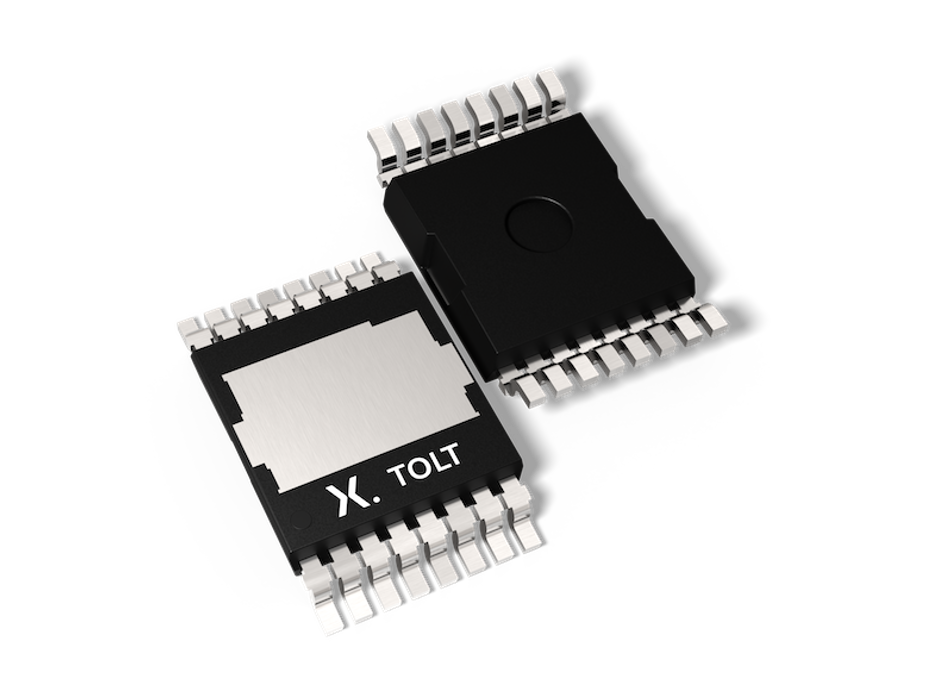
TOLT. Source: Nexperia
Application #5: LED Drivers, Audio, Robotics, and Consumer Adapters
Applications in the 80 to 650 V range include active-clamp and quasi-resonant flyback converters for adapters and LED drivers, LLC converters for compact power supplies, half-bridge Class-D audio stages, and three-phase inverter stages for small motors. These systems aim to prioritize high switching frequency to reduce magnetic size and improve power density in space-constrained designs. As frequency increases, switching losses, device capacitances, and reverse recovery behavior become dominant performance factors. As such, fast, low-loss wide bandgap devices like GaN are a strong solution.
Selection Guidance
For AC-DC adapters and LED drivers operating below 650 V, GaN FETs are generally the preferred switching technology. Their negligible reverse-recovery charge eliminates a major loss mechanism in CCM and active-clamp flyback converters, while their low gate charge reduces driver losses. Similarly, GaN’s low output charge supports fast switching transitions and higher operating frequencies. Increasing switching frequency reduces transformer and inductor size, directly improving power density and reducing enclosure size.
In Class-D audio amplifiers, GaN offers fast edge transitions and low switching losses, minimizing dead time and improving linearity at higher output power levels. Almost zero Qrr and low Qgd also determine low signal distortion and low THD at higher switching frequency. Reduced switching losses also minimize thermal stress, enabling compact amplifier designs without excessive heatsinking. In low-voltage robotics and small motor control systems, GaN enables higher PWM frequencies, reducing torque ripple and acoustic noise while improving efficiency at moderate current levels.
Performance Comparison
Silicon: MOSFETs are widely used in consumer power supplies due to cost advantages. However, reverse recovery losses and higher gate charge limit switching frequency and efficiency. As power density targets increase, these limitations become more pronounced. Qrr is limiting the switching speed and causing signal distortion at the zero crossing of the reference signal.
GaN: GaN devices offer a significant performance advantage in sub-650 V applications. The absence of body diode reverse recovery reduces switching energy and improves EMI performance. Lower QG x RDS(on) figure of merit supports higher efficiency and reduced magnetic size compared to silicon alternatives.
SiC: SiC MOSFETs are generally less advantageous in these lower-voltage, lower-power systems, as their voltage capability exceeds application requirements and their capacitance characteristics are less optimized for very high-frequency operation at sub-650 V. (I would remove this section since SiC is not used in the low voltage
Package Guidance
Compact form factor and thermal efficiency dominate package selection in consumer and lighting applications. Designers must meet strict height limits, minimize magnetic size, and maintain low EMI in densely populated PCBs.
For LED drivers, adapters, audio amplifiers, and compact robotic controllers operating at ≤650 V, GaN FETs in DFN, QFN, and CSP-style packages provide the strongest fit. These leadless packages minimize parasitic inductance in high di/dt switching loops, which reduces voltage overshoot and EMI. Their small footprint also enables shorter current paths and tighter gate-drive routing.
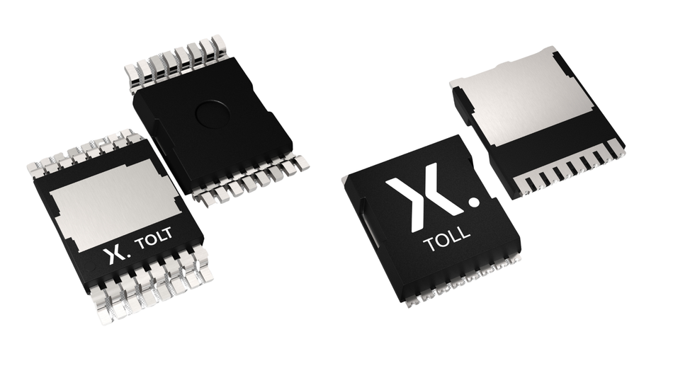
In higher-power LED lighting systems, gaming power supplies, or industrial control units approaching 650 V, surface-mount options such as TOLL/TOLT CCPAK GaN offer improved thermal performance over smaller DFN/QFN packages while preserving low-inductance switching paths. And, where designers require additional thermal headroom or higher voltage robustness near 650 V bus limits, D2PAK-7 SiC MOSFETs or SiC Schottky diodes offer greater voltage margin and strong heat dissipation through the PCB and external cooling structure.
Ultimately, the best approach is the TOP-side cooling for increasing power density and reducing the overall system form factor.
Application #6: Automotive Systems Requiring Qualified Devices
Automotive power systems span voltage domains from 48 V mild-hybrid architectures to 800 and 1200 V traction platforms. Applications include onboard charger PFC and DC-DC stages, traction inverter half- and full-bridge stages, 48 V inverter modules, battery management system (BMS) switching paths, and high-voltage-to-low-voltage (HV-LV) converters. These systems often have to contend with wide ambient temperature swings, mechanical vibration, and strict lifetimes that often exceed fifteen years. As a result, device selection must balance electrical performance with qualification level, process stability, and predictable long-term behavior.
Selection Guidance
Automotive environments demand devices that behave predictably across broad temperature ranges and under continuous thermal cycling. In high-voltage traction inverters, onboard chargers, and HV-LV converters operating at 800 V and above, 1200 V SiC MOSFETs provide the necessary voltage margin and thermal resilience. Stable RDS(on) behavior across temperature improves conduction efficiency under elevated junction conditions and supports sustained high-power operation. Controlled threshold voltage tolerance further enhances switching symmetry and reliable paralleling in inverter legs.
In 48 V subsystems and BMS switching paths, the requirements differ. Here, compact design, high PWM frequency, and low static loss are often prioritized over extreme voltage capability. GaN devices can enable higher switching frequencies with reduced switching energy, thereby improving power density in localized converters and relay-replacement circuits. Their fast transition capability also benefits BMS protection paths that require rapid response and minimal conduction loss.
Auxiliary automotive converters, including boost and rectification stages, benefit from SiC Schottky diodes. Their low forward voltage and negligible reverse recovery reduce switching losses and improve efficiency in high-frequency stages.
Performance Comparison
Silicon: Silicon devices are viable in cost-sensitive automotive functions but encounter limitations at high temperature and high switching frequency. Reverse recovery behavior and higher switching losses restrict their use in high-efficiency onboard chargers and traction inverter stages. They can be selected for low-end OBC but not in the main traction inverter and HVAC systems.
GaN: GaN devices perform effectively in 48 V conversion systems and high-frequency auxiliary stages. Their low switching losses and negligible reverse recovery support compact, efficient designs. However, voltage headroom constraints limit their suitability in 800 V traction or HV-LV systems in single-level solutions. More complex multilevel topologies are also starting to evaluate GaN switches in both OBC and main traction inverter sections.
SiC: SiC provides the strongest match for high-voltage and high-power automotive applications. It supports 800 to 1200 V operation with stable conduction characteristics across temperature and robust recovery behavior during hard-switched events.
Package Guidance
For traction inverter stages, onboard charger boost and DC-DC stages, and HV-LV converters, D2PAK-7 and TO-247-4 packages provide automotive-qualified solutions with strong thermal performance. In compact onboard charger modules and high-efficiency converters, top-side cooled packages such as X.PAK and QDPAK improve heat extraction and reduce PCB thermal stress.
In 48 V systems, BMS switching, and relay replacement circuits, low-voltage DFN and QFN packages can deliver compact layout, low parasitic inductance, and efficient thermal management.
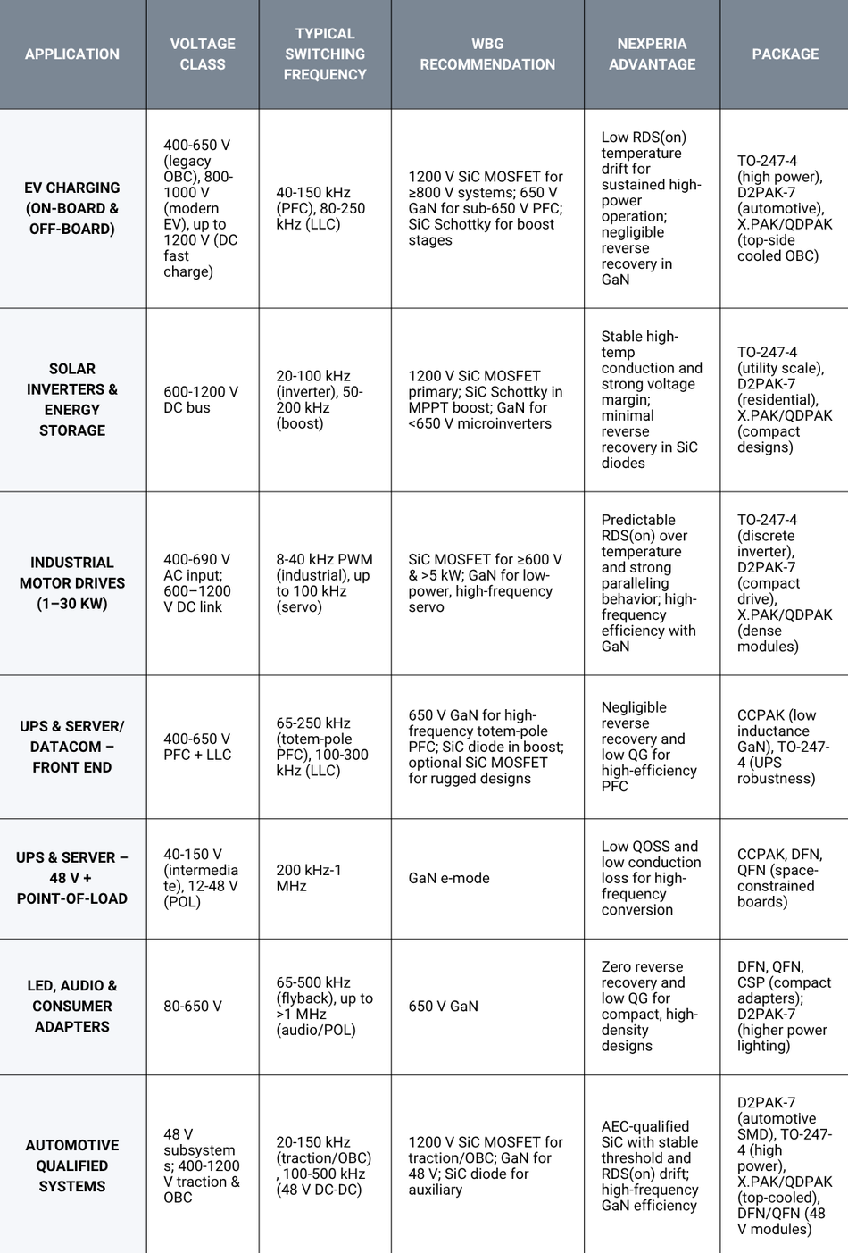
Decision Table
Conclusion
Wide bandgap device selection is fundamentally a system-level optimization problem. Designers must consider voltage class, switching frequency, load profile, thermal constraints, reliability requirements, and packaging strategy to choose the right device for the system.
SiC MOSFETs dominate high-voltage and high-power systems such as EV charging, solar inverters, and industrial drives. GaN FETs unlock high-frequency, density-focused architectures in server power supplies, adapters, LED drivers, and compact motor systems. SiC Schottky diodes complement both by reducing reverse recovery losses in boost and rectification stages.
By applying an application-first framework and evaluating parameters such as RDS(on) temperature stability, threshold voltage tolerance, gate charge balance, and packaging, engineers can confidently navigate the difficult decision choices. With a broad portfolio of WBG solutions, including industry-leading performance and packaging, and deep expertise in the field, Nexperia is helping customers navigate these challenges to design the next generation of power systems.