Maximizing Performance with JFETs in Medical Instrumentation
JFETs are uniquely positioned to maximize the performance of modern medical instrumentation.

28 May, 2025. 5 minutes read
Modern medical instrumentation demands signal integrity at extremely low levels. Certain medical devices, such as electroencephalography (EEG) and electrocardiography (ECG), rely on circuitry operating as low as the microvolt range. But the performance of medical devices can often be a matter of life or death. Performance compromises are not an option, even at such low voltages.
Amplifying these low-level signals presents a fundamental design challenge: mitigating sources of degradation such as noise, distortion, and input loading. Traditional bipolar and even CMOS solutions frequently introduce limitations in one or more of these areas. Junction Field-Effect Transistors (JFETs), however, are an optimal device for many front-end analog stages in medical applications.
With a unique combination of ultra-low gate leakage, low input capacitance, and excellent voltage noise performance, JFETs are uniquely positioned to maximize the performance of modern medical instrumentation.
Sensor Characteristics in Medical Applications
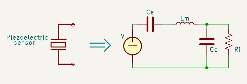
Many sensors used in medical instrumentation exhibit high output impedance, which places stringent demands on the design of the signal acquisition path. Piezoelectric accelerometers and hydrophones, for example, generate charge in response to mechanical deformation, while photodiodes used in pulse oximetry and optical heart rate monitoring convert light intensity into small current signals. Similarly, ECG and EEG electrodes detect biopotentials through skin-electrode interfaces that often exceed 1 MΩ in impedance.
These high-impedance sources pose multiple challenges. First, they are highly sensitive to input bias current. Any appreciable current drawn by the amplifier's input can develop significant voltage drops across the source and cause signal distortion or attenuation. Additionally, parasitic capacitance at the amplifier input can form unintended low-pass filters with the source impedance, limiting bandwidth and introducing phase distortion in time-critical measurements.
To interface effectively with such sources, amplifiers must meet three requirements. The first is high input impedance, typically in the GΩ range, to avoid loading the signal source and degrading signal amplitude. Second, ultra-low input noise current is needed to prevent noise from coupling through the high source impedance, which can dominate the overall system noise figure. Finally, low input capacitance is a must for preserving bandwidth and maintaining signal integrity across the entire frequency spectrum of interest.
Why JFETs Excel in Medical Analog Front Ends
JFETs offer a unique set of electrical characteristics that make them a great choice for the front-end amplification of weak, high-impedance signals in medical systems.
Gate Leakage and Noise Current Performance
A major performance advantage lies in their exceptionally low gate leakage current, typically less than 1 picoampere, which allows the use of high-value feedback resistors without introducing significant offset or noise. This is valuable in transimpedance amplifier configurations, such as those used with photodiodes and piezoelectric sensors. In these situations, low gate leakage allows for the circuit to maintain DC stability and low input bias current to preserve measurement integrity.
JFETs also produce extraordinarily low input noise current. Noise current is proportional to the square root of twice the product of the electron charge and gate current, as defined by the following equation.
in=2qI
Where
in is the shot noise current (A/√Hz)
q is the elementary charge (~1.602x10^-19 C)
I is the DC current through the junction. In this case, it’s the gate leakage current
That means that JFET’s sub-nanoampere gate currents translate to noise contributions in the femtoampere-per-root-Hertz range, which is practically negligible even with megohm-range sensor impedances. This behavior enables JFET-based circuits to maintain low total input-referred noise.
Voltage Noise and Capacitance Advantages
In addition to current noise performance, JFETs exhibit excellent voltage noise characteristics across the audio and low-kilohertz spectrum. Many biomedical signals, including ECG, EMG, and EEG, reside in this frequency range. With voltage noise densities below 2 nV/√Hz, well-designed JFETs can outperform many low-noise bipolar and CMOS alternatives, especially when high source impedance would otherwise translate current noise into voltage noise.
Low input capacitance (i.e., often just a few picofarads) is another advantage. This reduces bandwidth-limiting interactions with sensor impedance and minimizes capacitive loading, preserves fast transient response, and reduces the impact of noise gain in wideband or feedback-sensitive configurations.
Thermal Stability and Matching
JFETs also exhibit strong thermal stability, which is important in medical environments to minimize drift. In precision applications, matched JFET pairs can be used to construct differential stages with minimal offset voltage and excellent common-mode rejection. These characteristics make JFETs especially effective in diagnostic-grade instrumentation.
Circuit Architectures Using JFETs
While JFETs are a great choice for medical applications, their circuit architecture will ultimately define the performance of the system as a whole.
Charge Amplifiers for Piezo Sensors
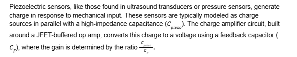
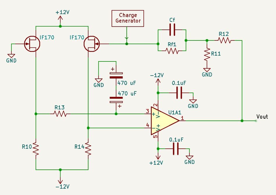
JFETs configured as source followers, such as InterFET’s IF170, provide a high-impedance buffer between the sensor and amplifier that minimizes loading and maintains fidelity. To ensure amplifier stability, resistor pairs like R5 and R6 are inserted in the feedback path to control phase margin. This mitigates the phase shift caused by capacitive loading and prevents oscillation in high-gain or unity-gain configurations.
Photodiode Transimpedance Amplifiers
Photodiodes are used in pulse oximetry and optical sensors and require low-noise transimpedance amplifiers (TIAs) to convert current into voltage. High-impedance photodiodes are sensitive to input bias current and capacitance. Placing a JFET source follower, like InterFET’s IF170 or IF389, in front of the op amp dramatically lowers effective input capacitance and noise current seen by the photodiode. This improves both frequency response and signal-to-noise ratio.

Instrumentation Amplifiers with JFET Front-Ends
Electrophysiological measurements such as ECG and EEG benefit from JFET-input differential buffer stages due to their high input impedance, low noise, and balanced signal handling. The IF389 dual JFET is well-suited for this purpose, offering tight VGS matching and low gate leakage. When configured as a differential pair, it serves as a front-end buffer to a traditional op-amp-based instrumentation amplifier to enhance input common-mode rejection and minimize offset drift. Symmetrical layout and thermal coupling of the two JFETs further improve matching and performance, enabling robust detection of µV-level bioelectric signals.
Practical Design Considerations
Designing with JFETs in medical instrumentation requires attention to several practical aspects to maintain signal integrity and ensure long-term stability.
Stability and Frequency Response
JFET stages, particularly when used as high-impedance front ends in transimpedance or charge amplifier circuits, are susceptible to phase margin degradation. The combination of high feedback resistance and input capacitance can create significant phase shift at higher frequencies, risking oscillation. To counter this, resistive dividers or source degeneration resistors can be used to control gain and bandwidth.
In addition, capacitive equalization networks are often inserted in feedback paths to cancel capacitive roll-off and extend frequency response. These networks are designed to balance the pole formed by the input and feedback capacitance to maximize bandwidth without compromising stability.
PCB Layout and Leakage Control
Due to the ultra-high input impedance of JFET gates, circuit layouts must minimize leakage currents and parasitic capacitance. Board contamination, such as flux residue or moisture, can lead to picoamp-level leakage that distorts low-level signals. Guard rings tied to the same potential as the gate, placed around sensitive traces, can intercept leakage currents and provide electrostatic shielding. Using solder mask openings to isolate high-impedance nodes and employing low-dielectric materials can further reduce parasitic effects.
Power Supply and Biasing Techniques
JFETs require careful biasing to maintain optimal transconductance and noise performance. This is often accomplished using current source loads or resistive voltage dividers, filtered to eliminate power supply ripple that could couple into sensitive signal paths. Because JFETs are compatible with a wide range of supply voltages, they can operate from dual rails in analog systems or from 48V phantom power, as found in medical-grade condenser microphones. Ensuring quiet and stable biasing is central to unlocking the full precision of JFET-based analog front ends.
Conclusion
In medical instrumentation, accuracy at the microvolt level can influence life-critical decisions. JFETs offer a rare combination of traits that align directly with the demands of high-impedance, low-amplitude sensor interfaces and elevate the performance of front-end circuitry beyond what is possible with bipolar or CMOS alternatives. With proper circuit architecture and layout, JFETs can unlock systems that deliver reliable data so that doctors can make life-saving decisions.