Compact LiDAR Systems Powered by Low-Profile Pulse Laser Diodes For Automation Applications
Enabling precision, efficiency, and miniaturization in industrial automation through advanced photonics.

04 Jun, 2025. 8 minutes read
Smart manufacturing utilizes integrated, intelligent technologies like the Internet of Things (IoT), artificial intelligence (AI), and robotics to optimize manufacturing processes through automation and real-time data analytics. At the heart of these cutting-edge advancements are photonics technologies, which utilize light-based mechanisms to advance manufacturing capabilities. Essential to modern production environments, photonics enhances sensing, processing, and inspection tasks.
According to the Fortune Business Insights report titled “Photonics Market Size, Share & COVID-19 Impact Analysis,” the global photonics market size is projected to grow from USD 983.51 billion in 2024 to USD 1,642.61 billion by 2032 at a CAGR of 6.7% [1]. This growth underscores the expanding role of photonic components in modern industrial systems.
A critical innovation within this domain is the development of compact Light Detection and Ranging (LiDAR) systems. These systems, particularly those powered by low-profile pulse laser diodes, are pivotal in areas requiring high precision and responsiveness such as robotics, quality control, and autonomous material handling. Compact LiDAR systems are prized for their ability to offer miniaturization, reduced power consumption, and superior accuracy—qualities that are indispensable for the advancement of manufacturing automation.
This article explores the transformative influence of photonics in smart manufacturing, focusing on the deployment of compact LiDAR systems. It details their pivotal applications, delineates their competitive advantages, addresses implementation challenges, and forecasts future trends that will shape the industry.
Photonics in Smart Manufacturing
Photonics refers to generating, manipulating, and detecting photons, particularly in the visible and near-infrared spectrum, to perform various functions of utmost importance in smart manufacturing. These advanced optical systems enable high-speed real-time monitoring through optical sensors while facilitating precision material processing applications, including cutting, welding, and engraving.
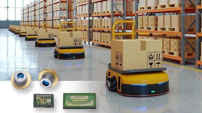
Among the most impactful implementations is LiDAR technology, which provides essential 3D mapping and quality inspection capabilities. Compact LiDAR systems utilizing low-profile pulse laser diodes offer advantages, delivering high-accuracy depth perception even in space-constrained industrial environments. Their combination of high-frequency operation and minimal power requirements makes these systems exceptionally well-suited for integration into automated production lines, where they enhance both precision and efficiency. These capabilities are integral to the design of cyber-physical production systems, one of the core components of Industry 4.0.

Applications of Compact LiDAR Systems in Smart Manufacturing
Compact LiDAR systems have enabled various photonics applications to become more accessible, mobile, and adaptable. Their incorporation into various segments of the manufacturing process illustrates their versatile utility.
Sensing and Data Acquisition
The compact LiDAR system's most impactful application is in real-time, high-resolution sensing. LiDAR technology works by emitting short laser pulses and measuring the time it takes for these pulses to reflect off surfaces and return to the detector. Low-profile pulse laser diodes in such systems enable high pulse repetition rates, compact form factors, and reduced energy consumption.
In smart manufacturing, these systems are used extensively in robotic navigation, object detection, and production line mapping. Their compactness ensures they can be mounted on mobile platforms such as autonomous guided vehicles (AGVs), enabling dynamic mapping and obstacle avoidance in factory environments. The high spatial resolution provided by LiDAR improves feedback accuracy for closed-loop control, resulting in enhanced system responsiveness.
Laser-Based Processing
While LiDAR is primarily a sensing technology, its laser foundation aligns with broader laser-based processing techniques in manufacturing. Compact LiDAR systems, integrated alongside laser machining tools, contribute to real-time monitoring and adaptive control of material processing tasks such as micro-welding or additive manufacturing.
Overlaying a LiDAR-based spatial map with the target surface enables the processing laser to adapt to real-time topographical changes, ensuring consistent processing even when the material or workpiece exhibits irregularities. This approach reduces defects and supports inline adjustments, ultimately contributing to higher process reliability.
Imaging and Quality Control
Compact LiDAR systems also enhance machine vision and quality assurance protocols, combining depth mapping with conventional 2D imaging to enable comprehensive inspections that consider surface geometry alongside texture and colour.
For example, in the automotive and electronics industries, compact LiDAR facilitates micro-warping detection in printed circuit boards or misalignment in component assemblies. Using pulse laser diodes ensures fast data acquisition, thereby maintaining throughput without sacrificing accuracy.
Advantages of Compact LiDAR Over Traditional Systems
Integrating compact LiDAR systems into photonics-driven manufacturing environments provides several strategic advantages:
Enhanced Spatial Precision:
LiDAR systems provide centimetre to millimetre-level resolution, essential for high-precision applications such as electronic component assembly or semiconductor inspection.
Scalability:
The low-profile design of compact LiDAR modules enhances their scalability, allowing for seamless integration into various applications, from compact robotic joints to larger metrology systems. This flexibility offers a significant advantage over traditional, bulky equipment, enabling LiDAR systems to be scaled up or down based on the specific requirements of the task or environment.
Real-Time Monitoring and Adaptability:
LiDAR systems can dynamically track object movement and surface variations, unlike static sensors. Their use in adaptive systems ensures consistency despite variability in manufacturing conditions.
Reduced Maintenance and Operational Downtime:
Compact LiDAR modules have few moving parts and can be sealed against dust and contaminants. This durability contributes to extended operational lifespans and lower total cost of ownership compared to traditional optical or mechanical sensing tools.
Energy and Resource Efficiency:
Pulse laser diodes operate with high electrical-to-optical conversion efficiency. This translates to lower power requirements, which are especially crucial in distributed systems and mobile robotic units.
Challenges and Solutions
Despite their potential, compact LiDAR systems face several implementation challenges. Addressing these is key to unlocking their full value in smart manufacturing.
Environmental Robustness
Manufacturing environments are often harsh, involving dust, vibration, and thermal fluctuations. Compact LiDAR systems, although inherently robust due to fewer mechanical parts, must be further optimized through hermetic sealing, vibration damping, and temperature compensation mechanisms. Research into ruggedized optical materials and integrated thermal regulation continues to address this limitation.
System Integration
Compact LiDAR into existing factory infrastructure requires alignment with industrial communication protocols (e.g., OPC UA, Modbus) and compatibility with manufacturing execution systems (MES). Vendors increasingly offer LiDAR modules with built-in interfaces and APIs to ease integration challenges. Further, plug-and-play capabilities and modular architectures are facilitating retrofitting into legacy systems.
Technology Integration and Optimization
Compact LiDAR performance depends on precision components, primarily Pulse Laser Diodes (PLDs) and optical sensors:
Pulse Laser Diodes emit nanosecond-range light pulses, providing the core signal for time-of-flight measurements. Their characteristics (peak power, repetition rate, and jitter) directly influence range and spatial resolution. Newer low-profile PLDs, like those from Hamamatsu, deliver high peak power (100W) with reduced form factor and energy demand ideal for embedded industrial systems.
Optical Sensors such as avalanche photodiodes (APDs) and single-photon avalanche diodes (SPADs) are used to detect returned pulses. These advanced photodetectors offer superior sensitivity and timing precision, essential for high-resolution depth mapping in dynamic manufacturing environments.
These technologies not only ensure reliable object detection and mapping but also enhance adaptability across varying surface textures and ambient lighting conditions. Improvements in packaging, thermal stability, and signal amplification further contribute to durability and accuracy.
Data Volume and Processing
High-frequency LiDAR scanning generates large volumes of spatial data. Efficient data handling and fusion with other sensor modalities (e.g., vision systems and tactile sensors) remain key concerns. Integration with edge computing hardware and real-time data processing algorithms, including machine learning for feature extraction, can alleviate computational bottlenecks and support intelligent decision-making.
Initial Capital Costs
While the cost of LiDAR has declined significantly in recent years due to advancements in diode and packaging technologies, initial procurement can still be substantial. However, the long-term return on investment through improved process efficiency, defect reduction, and automation scalability often justifies the expenditure.
Advances in High-Speed Laser Diodes
The trajectory of compact LiDAR systems indicates their increasing role as essential components within intelligent manufacturing and robotics platforms. As the demand for precision, efficiency, and adaptability grows, several key technological trends are anticipated to shape the next development phase, areas in which Hamamatsu Photonics’ optoelectronic innovations can offer enabling value.
The continued refinement of pulsed laser diodes with high peak power, low jitter, and nanosecond-range pulse widths is central to enhancing the responsiveness of LiDAR systems. Such characteristics facilitate precise time-of-flight measurements and support integration with motion control frameworks in advanced robotics. Hamamatsu’s portfolio of pulsed laser diodes is well-suited for such time-critical applications, providing core components for the next generation of compact sensing modules.
Photonics-Integrated Miniaturization:
The photonic integration trend enables LiDAR systems to become smaller, more robust, and cost-effective. While full photonic integrated circuits (PICs) are evolving in parallel domains, Hamamatsu’s work on compact packaging of photonic components such as semiconductor laser modules and detectors supports the miniaturization efforts needed in space-constrained or embedded industrial applications[8].
System Readiness for Intelligent Platforms:
Emerging LiDAR modules are increasingly expected to interface seamlessly with intelligent systems for real-time monitoring, data fusion, and adaptive decision-making. Although system integrators often handle the interpretative layer, the stability and precision of Hamamatsu’s light sources and photodetectors make them suitable for deployment in AI-augmented platforms, requiring reliable data acquisition and temporal consistency[9].
Sustainability in Manufacturing:
Compact, energy-efficient LiDAR components contribute to the overarching goals of green manufacturing by enabling fine-grained monitoring, resource optimization, and predictive maintenance. Hamamatsu’s emphasis on component durability, thermal efficiency, and low power consumption aligns well with the principles of sustainable system design[10].
Global Standardisation and Interoperability:
International efforts to develop interoperability frameworks for LiDAR deployment in industrial environments pave the way for broader adoption. Hamamatsu's optoelectronic components' design consistency and signal reliability make them viable candidates for inclusion in modular, standards-aligned architectures that demand repeatability and cross-platform integration[9].
Key technologies: The advantages of PLD in compact LiDAR systems
Low-profile pulse laser diodes (PLDs) offer several advantages for compact LiDAR systems:
High Peak Power: These PLDs can achieve peak powers exceeding 100W,sufficient for precise distance measurement in industrial environments .
Energy Efficiency: Their design enables low power consumption, supporting extended operation in compact and battery-powered platforms. Compact Design: The low-profile SMD format enables the creation of smaller, more compact LiDAR systems, which are easier to integrate into various applications.
Mass Production: The compatibility with wafer-level manufacturing allows for large-volume production, reducing costs and improving scalability.
Durability: These PLDs are resin-embedded for enhanced durability and longer lifetimes.
High Photon Detection Efficiency: Improved photon detection efficiency ensures better performance in detecting and mapping objects.
These advantages make low-profile PLDs ideal for applications requiring precise, efficient, and compact LiDAR systems.
Conclusion
Fusing compact LiDAR systems, especially those utilizing low-profile pulse laser diodes with photonics technologies, transforms smart manufacturing. These systems deliver unprecedented accuracy, real-time adaptability, and spatial awareness, which are critical for achieving the responsiveness and efficiency demanded by Industry 4.0 paradigms.
While challenges persist regarding integration, robustness, and data processing, recent advancements in pulse laser diode (PLD) efficiency, high-sensitivity photodetectors (such as APDs and SPADs), and miniaturized optical packaging continue to mitigate these hurdles. Furthermore, the adoption of edge computing modules, standardized industrial communication interfaces, and modular sensor architectures supports seamless deployment.
These enabling technologies pave the way for the widespread integration of compact LiDAR as a standard tool in intelligent factories—empowering agile production lines, self-aware machines, and high-quality outputs with reduced environmental impact.
Call to Action
Stakeholders in industrial automation must recognize the strategic advantage of compact LiDAR technologies. Organizations can position themselves at the forefront of smart manufacturing innovation by investing in research, fostering partnerships, and staying current with technological developments. Active engagement with standards bodies, educational initiatives, and pilot deployments will accelerate the effective deployment of photonics-enabled manufacturing solutions.
Manufacturers and technology providers such as Hamamatsu Photonics, known for developing pulsed laser diodes, offer components that may be considered when designing and implementing compact LiDAR systems. Staying informed about commercially available technologies can support more informed decision-making and system design.
References and further reading
[1] Fortune Business Insights, "Photonics Market Size, Share & COVID-19 Impact Analysis," [Online]. Available: https://www.fortunebusinessinsights.com/photonics-market-106525.
[2] B. E. A. Saleh and M. C. Teich, Fundamentals of Photonics, 3rd ed. Wiley-Interscience, 2007.
[3] J. Zhang and S. Singh, "LOAM: Lidar Odometry and Mapping in Real-time," Robotics: Science and systems. Vol. 2. No. 9. 2014.
[4] P. Rainbow, "High-power pulsed laser diodes take on new industrial and commercial applications," Photonics Spectra, vol. 38, pp. 105–108, 2004.
[5] Hamamatsu Photonics, "Pulsed Laser Diodes," [Online]. Available: https://www.hamamatsu.com/jp/en/product/lasers/semiconductor-lasers/plds.html
[6]. M. P. Mollah et al., "Efficient compression method for roadside LiDAR data," in Proc. 31st ACM Int. Conf. on Information & Knowledge Management (CIKM), 2022, pp. 3726–3730.
[7] M. Smit et al., "An introduction to InP-based generic integration technology," Semiconductor Science and Technology, vol. 29, no. 8, 2012.
[8] Photodiodes. Hamamatsu Photonics K.K. [Online]. Available: https://www.hamamatsu.com/jp/en/product/optical-sensors/photodiodes.html.
[9] Optical Sensors. Hamamatsu Photonics K.K. [Online]. Available: https://www.hamamatsu.com/jp/en/product/optical-sensors.html.
[10] Environmentally Contributing and Friendly Products (2021). Hamamatsu Photonics K.K. [Online]. Available: https://www.hamamatsu.com/jp/en/ourcompany/sustainability/environment/environmentally-contributing-and-friendly-products/2021.html.