Accelerating the Adoption of Chiplet-Based Semiconductor Architectures
The ForwardEdge ASIC (FEASIC) UCIe IP advances the deployment of interoperable chiplet-based systems.

04 Aug, 2026. 4 minutes read
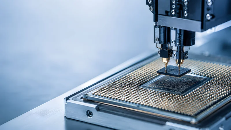
The semiconductor industry is increasingly adopting a chiplet-based architecture as a practical solution to the growing complexities, costs, and scalability challenges associated with traditional monolithic integrated circuits.
With the increasing price of advanced process nodes and longer design cycles, semiconductor companies are investigating new options for delivering higher performance, more flexibility, and faster product development. One of the most successful solutions has been the rise of chiplet technology, empowering complex systems to be built from multiple specialized dies in a single package.
The critical enabler for this design shift is efficient communication between individual chiplets. High-performance/low-power die-to-die interconnects are essential to make a multi-chip package operate as a single system, not a set of separate components.
This need has led to the advent of Universal Chiplet Interconnect Express (UCIe), an open industry standard that ensures high-bandwidth, low-latency, low-power communication between chiplets. FEASIC’s UCIe IP solution fulfills this need with a full implementation of the UCIe-SP standard package architecture, permitting developers to accelerate the deployment of interoperable chiplet-based systems.
Chiplet Architectures on the Rise
For decades, semiconductor innovation meant putting more functionality on a single die. This has resulted in large performance gains but has likewise become increasingly complex to maintain. Manufacturing large monolithic chips is also difficult and can result in low yield, high fabrication cost, long development time, and high design complexity.
Chiplet architecture provides a fundamentally different approach. Instead of building a single large die, engineers can split a system into smaller functional dies. Each of them can then be tuned for a particular job. Processor cores, AI accelerators, memory controllers, networking interfaces, and analog functions can be developed independently and then integrated into a common package.
There are several advantages to this modular design philosophy. Smaller dies generally improve yields and reduce overall costs of production. Individual chiplets can also be reused across multiple products, which shortens development timelines and improves return on investment. Moreover, designers can combine technologies fabricated with different process nodes, so that each function can be realized with the most appropriate manufacturing technology. Each chiplet is allowed to progress at its own desired pace, which allows upgrading specific or critical parts of the design independently. The overall packaged product can then improve incrementally at a much lower cost.
But the success of this approach depends on how well these chiplets can communicate with each other. Without a common communication framework, chiplet ecosystems are at risk of fragmenting due to proprietary interfaces and limited interoperability.
This modular approach is also reshaping the broader chiplet ecosystem. Reusable components can now be developed once and integrated across multiple platforms, echoing how standardization and modular design transformed other segments of the technology industry.
Rather than designing and fabricating every subsystem in-house, companies can source specialized chiplets from different suppliers and integrate them into application-specific solutions, fostering innovation, reducing development costs, and speeding up product launches. UCIe addresses these problems directly, offering a standardized foundation for chiplet interoperability.

UCIe: The Foundation for Chiplet Interoperability
UCIe was created to address the interoperability issue that comes with chiplet adoption. The standard establishes a common die-to-die communication framework that allows chiplets from different vendors, foundries, and process technologies to cooperate in the same package.
UCIe defines standardized physical, protocol, and software interfaces that eliminate many of the barriers that have traditionally made heterogeneous integration difficult. Instead of being forced to develop custom interconnects for each design, semiconductor designers can now leverage a common ecosystem supported by multiple industry players.
This is particularly true for emerging applications that must move massive amounts of data between compute, memory, and accelerator resources. Efficient communication between multiple functional blocks is a key requirement for artificial intelligence workloads, high-performance computing systems, data center processors, and advanced edge-computing platforms. UCIe allows such systems to achieve high bandwidth density with low latency and power consumption.
UCIe extends proven high-speed interconnect design principles to the package level, easing integration and allowing existing design methodologies to carry over to chiplet-based systems.
FEASIC UCIe IP Solution
ForwardEdgeASIC (FEASIC) has built a complete UCIe IP implementation that offers the basic infrastructure required for standards-compliant die-to-die communications. Instead of just offering individual building blocks, the company offers the complete UCIe stack, including the physical layer (PHY), die-to-die adapter functionality, and protocol support.
This off-the-shelf solution enables customers to incorporate UCIe connectivity into their designs without the huge effort required to engineer a custom interconnect architecture. With a pre-validated solution, development teams can innovate on features specific to the application, while lowering the risk associated with implementations.
The physical layer has been designed on the GlobalFoundries 12LP+ process technology and tuned for performance and power efficiency. FEASIC implementation supports x16 connectivity and provides transfer rates of up to 16 GT/s per lane to meet the high aggregate bandwidth required by today’s data-intensive applications.
A key differentiator is that the solution has already been validated in the laboratory. And as the chiplet ecosystem matures, proven implementations gain value, as they reduce uncertainty in system integration and shorten qualification timelines.

Future Outlook
One of the biggest trends in modern chip design has been the move from monolithic semiconductor devices to modular chiplet architecture. As demand increases for artificial intelligence, machine learning, cloud computing, networking, and edge-processing applications, the ability to efficiently integrate multiple specialized dies in a single package will become increasingly important.
UCIe provides the standardized foundation to turn this vision into reality. The standard enables high-speed, low-latency communication between chiplets, permitting developers to realize the full benefits of modular semiconductor design.
FEASIC’s UCIe IP solution is a practical implementation of this technology, offering designers a validated and ready-to-deploy interconnect platform. It supports high-bandwidth communication, heterogeneous integration, and scalable multi-die architectures to help accelerate the industry’s transition to a more flexible and interoperable chiplet ecosystem.
With semiconductor complexity continuing to grow, standardized die-to-die connectivity will be critical to the success of future generations of computing platforms. Solutions like FEASIC’s UCIe IP are helping to transition chiplets from an emerging concept to a core technology for next-generation semiconductor innovation.