A Physicist's Approach to Semiconductor Manufacturing
Physics is about the web, rather than the spider.

17 Apr, 2026. 5 minutes read

Physics studies nature in general. The fundamental basis of physics is based on repeatable observations, which leads to knowledge being built. In semiconductor manufacturing, this translates into a deep understanding of the “related” parameters in addition to the main goal of a specific operation.
Creating an IC is a sequential process where hundreds to a few thousand steps are used in sequence from concept/design/verification/manufacturing/tests/packaging to achieve something that works most of the time. This sequential process is a web of interactions that are dictated by first principles. Understanding the relevance of these interactions helps guide the team to the best possible outcome.
Working in this manufacturing environment is most effective when first principles are used to build a manufacturing sequence for a given system, but first principles also define the entire system.
These constraints are tightly coupled. A change in doping concentration influences electric fields, which in turn affect breakdown behavior. Layout decisions shape parasitic effects, while process variations alter performance and yield. None of these factors operate in isolation. Each propagates through the system; it’s very much like pulling one node of a spiderweb ultimately moves the whole web.
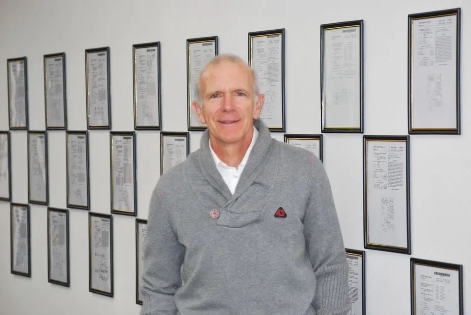
SimpleChips’ founder and CEO, Alain R. Comeau built his career on a physics foundation. He observed that characteristics of physicists, which are really helpful in the industry, include:
- Deep understanding of what is possible
- Technical flexibility
- Endless curiosity
- Perspective of technical landscape
- Global picture
- Good sense of observation
- Need for understanding
From Physics to Fabrication
Educated in solid-state physics at the University of Sherbrooke, Quebec, M. Comeau entered the industry through yield engineering and process integration at Mitel Semiconductor. Yield engineering focuses on identifying the physical origins of device failure and variation, tracking observed behavior back to underlying mechanisms.
Process integration adds another layer of complexity. It requires coordinating multiple fabrication steps—implantation, diffusion, deposition, and etching—while ensuring that the resulting device structure behaves as intended. Each step introduces constraints, and each interaction carries consequences.
In this context, problems are rarely localized. A yield issue observed at test may originate from a subtle interaction between process steps several layers earlier. Similarly, a reliability concern may trace back to electric field distribution shaped by layout decisions. Even a performance deviation may reflect material behavior under specific material, thermal or electrical conditions.
Addressing these issues requires a mindset that does not isolate variables prematurely but instead traces cause and effect across domains. This is where a physics background becomes operational.
Rather than treating fabrication and design as separate concerns, a physics-driven approach connects them through underlying principles. Device behavior becomes something to be understood and anticipated during design and process definition rather than an outcome to be measured only after fabrication.
Bridging Design and Manufacturing
Throughout his career, M. Comeau worked in roles that reinforced this perspective. From process integration and yield problem resolution to technology transfer across fabs and advanced device development, his work consistently involved systems where multiple variables interact simultaneously.
Technology transfer, for example, is not a procedural exercise. Moving a CMOS process from one fabrication facility to another involves differences in equipment, materials, environmental conditions, and process control. Even small changes can lead to measurable differences in device behavior and yield. Ensuring consistency requires understanding the physics that governs their outcomes.
Similarly, work on silicon avalanche photodiodes or surge protection devices involves managing high electric fields, breakdown mechanisms, and reliability constraints under extreme conditions. These are not problems that can be solved through incremental adjustment alone. They require a clear understanding of how devices behave at their limits.
Over time, this kind of exposure builds a distinctive form of expertise, grounded in the ability to interpret behavior, identify root causes, and navigate complex interactions with clarity. Patterns emerge, failure mechanisms become recognizable, and solutions can be evaluated for both immediate effectiveness and long-term stability.
This depth becomes particularly valuable at the boundary between design and manufacturing. In many organizations, these domains are separated structurally and operationally:
Design teams focus on circuit performance and functionality.
Manufacturing teams focus on yield, repeatability, and process control.
Communication between the two is often iterative, with issues discovered after fabrication and addressed through successive design or process modifications. This separation introduces friction. Design decisions may not fully account for process constraints, and manufacturing limitations may not be visible during early design stages. As a result, development cycles extend, and compromises accumulate.
A physics-based perspective aligns both domains through the same underlying principles, allowing constraints to be addressed during design rather than after fabrication. Trade-offs can be evaluated within a unified framework that considers device behavior, process variability, and system requirements simultaneously.
At SimpleChips, this integration is treated as a starting point, shaping how projects are approached from the outset. Design choices are considered in direct relation to fabrication realities, with device structures evaluated alongside process capabilities. Reliability and yield are embedded within the design itself, reducing iteration cycles, improving predictability, and reframing how problems are approached.
Experience as a System-Level Advantage
The trajectory of M. Comeau’s work illustrates how this perspective translates into device-level and process-level solutions.
In high-voltage device design, controlling breakdown behavior is not a matter of selecting a target voltage and scaling geometry. It requires shaping electric fields across the device so that breakdown occurs in a controlled and repeatable manner. This involves careful definition of junction profiles, doping gradients, and layout structures that distribute field intensity without introducing localized stress points.
Several of Alain’s patented designs address this class of problem, introducing device structures that manage electric field distribution and improve robustness under high-voltage conditions. Examples include US7701148B2, “HIGH VOLTAGE CURRENT SPLITTER AND METHOD,” and US10615132B2, “INTEGRATED CIRCUIT CAPABLE OF OPERATING AT VERY HIGH VOLTAGE AND MЕТHOD OF FABRICATING SAME.”
A similar level of system awareness appears in work on avalanche-based components. Devices operating in avalanche regimes depend on stable carrier multiplication under high electric fields. Small variations in material properties or geometry can shift breakdown characteristics, introduce noise, or reduce long-term reliability. Designing for stability in these conditions requires anticipating how the device will behave across variations in process and temperature.
This is where fabrication experience becomes inseparable from design.
In process integration and yield engineering, problems often present themselves far from their origin. A yield loss observed at electrical testing may trace back to implant conditions, diffusion behavior, or subtle interactions between process steps. Resolving such issues requires reconstructing the sequence of physical transformations that led to the observed behavior.
M. Comeau’s work across multiple fabs shows that fabrication and design operate as a single system. Variations in process conditions directly shape device behavior, requiring design decisions to account for how those variations manifest in silicon.
Across such domains as high-voltage IC design, avalanche devices, yield optimization, and process transfer, the same method is applied, aligning device structure, process conditions, and operating requirements so that behavior remains stable across variation and over time.
This is how experience accumulates as a system.
From Device Physics to Company Design
A physicist’s way of thinking begins with identifying governing mechanisms, understanding how they interact, and following their effects through the system. That perspective extends beyond devices and processes into how the company itself is structured.
At SimpleChips, decisions remain closely tied to technical understanding, and the boundary between design and manufacturing is minimized. Project selection reflects the same principle, focusing on problems where depth of understanding can be applied effectively under real constraints.
In semiconductor devices, behavior depends on how internal relationships are defined and controlled, from electric field distribution to material properties and process variation. Stability emerges when these elements remain coherent under operating conditions.
At the organizational level, technical capability, resource allocation, and decision-making must remain aligned for the company to operate effectively in a domain where constraints are tightly coupled, and outcomes depend on how well interactions are understood.
M. Comeau’s career reflects this continuity. The same approach used to interpret device behavior and resolve fabrication challenges is applied to how the company evolves: grounded in fundamentals, attentive to interactions, and structured to remain coherent under real-world conditions.
This is what allows a physicist to move from analyzing devices to building a company without changing the underlying method.
The domain changes. The system does not.