A Great Idea Is Not Yet a Product: XIVER on Industrializing Integrated Photonics Innovations
XIVER's Sreekanth Chirayath on why photonic innovations fail on the production line and how designing for manufacturing from the start changes the outcome.

15 Jul, 2026. 8 minutes read
Building Integrated Photonic Products That Scale
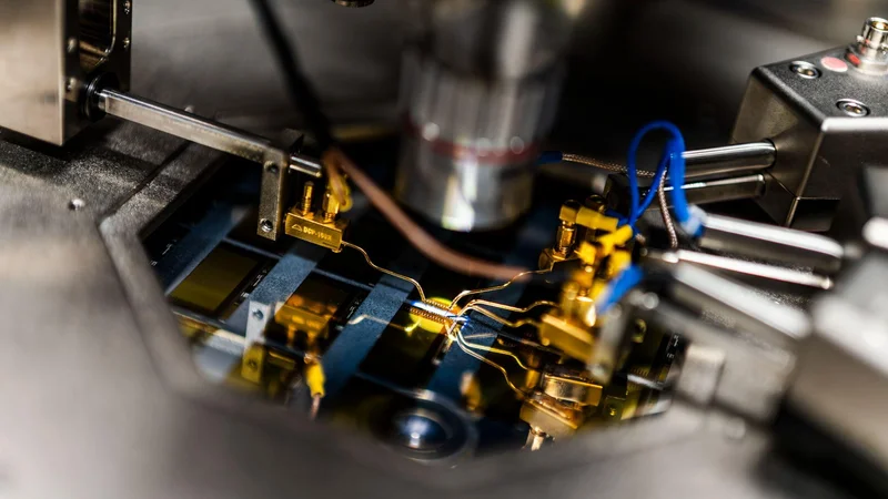
Integrated photonics has produced some of the most remarkable engineering achievements of the past decade. Yet for every photonic innovation that reaches the market, many more stall somewhere between the laboratory and commercial reality.
This gap, often called the valley of death, is not a failure of ideas but rather a failure of industrialization. A device that performs brilliantly on a handful of prototype wafers may behave very differently when manufactured at scale. Yield drops, process variations compound, timelines stretch, and the assumptions baked into a design optimized for demonstration begin to crack under the demands of production.
Bridging that gap requires more than engineering excellence. It demands that manufacturing be treated as a design constraint from day one. In this conversation, Sreekanth (Sree) Chirayath, Vice President Business Development at XIVER, explains what that looks like in practice and why the most successful integrated photonics teams are the ones that think about scale before they think they need to.
Innovation to Industrialization in Integrated Photonics: Insights from XIVER
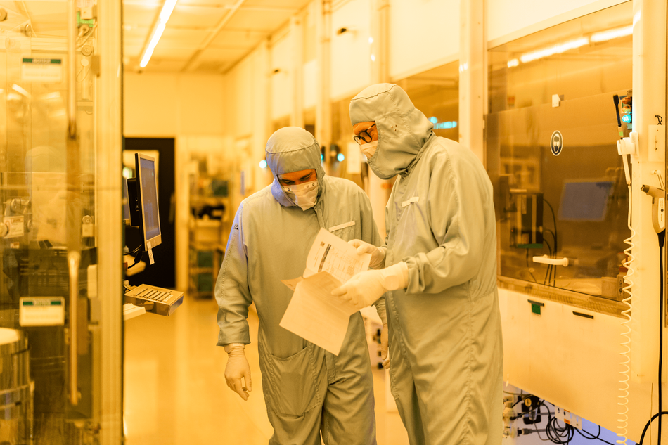
XIVER is a European-owned specialty microsystems and semiconductor foundry with more than 40 years of experience and a fully qualified 200 mm wafer fab at High Tech Campus Eindhoven. XIVER helps customers transform complex innovations into manufacturable, high-performance products by combining expertise in silicon micromachining, wafer-level processing, microsystems integration, and Design for Manufacturing (DfM). Core focus areas include semiconductor equipment and metrology, integrated photonics, advanced transducer technologies, and infrared sensing.
XIVER serves a diverse range of markets, including semiconductor equipment, integrated photonics, IR sensing, defense, and medtech. What differentiates XIVER is their concurrent engineering approach: the company works with customers from the earliest stages of development through industrialization and high-yield volume production. By combining agility, reliability, and manufacturing excellence, XIVER helps organizations accelerate time-to-market and successfully scale advanced technologies from concept to commercial reality.
Sreekanth (Sree) Chirayath, Ph.D., is Vice President Business Development at XIVER, focused on integrated photonics. With a background in physics, photonics, and semiconductors, he helps customers bridge the gap between innovation and manufacturing, supporting the industrialization of integrated photonic technologies for optical communications, sensing, AI infrastructure, and other high-growth applications.
Peter (PhotonDelta): There's an assumption in deep-tech circles that if you build something technically superior, the rest will follow. In your experience, what actually stops great technology from reaching the market?
Sree (XIVER): One of the biggest misconceptions in deep tech is that technical superiority alone guarantees commercial success. Many breakthrough technologies never reach the market because they fail to cross what we call the industrialization gap. A device may work perfectly on a handful of prototypes, but when you try to manufacture hundreds or thousands of wafers, yield issues emerge. Small process variations can significantly impact performance, creating unacceptable costs or reliability risks.
That is why our role as a specialty foundry extends beyond fabrication. We work closely with customers from the earliest stages to ensure that process choices, design decisions, and integration strategies are aligned with high-yield production from day one. By combining expertise in silicon micromachining, wafer-level processing, microsystems integration, and manufacturing, we help customers de-risk the transition from innovation to volume production. Great technologies reach the market not only when they perform exceptionally, but when they can be manufactured reliably, repeatedly, and economically on scale. That's where many innovations succeed or fail.
Peter (PhotonDelta): What are XIVER's core areas of expertise, and what kinds of challenges are customers typically looking to solve when they come to you?
Sree (XIVER): Customers generally come to us when they have a technically demanding microsystem, photonics or semiconductor challenge and need a partner that can turn an innovative concept into a reliable, manufacturable product.
Our core expertise is built around micromachining, wafer-level processing, microsystems integration, and DfM. Combined with our fully qualified 200 mm wafer fab, this capability allows us to support customers all the way from concept development and process design through industrialization and high-yield production.
At XIVER, we focus our business on three strategic domains where we see the strongest fit between market demand and our capabilities.
The first area is semiconductor and metrology equipment, which today represents roughly two-thirds of our business. Here, customers are often developing precision measurement systems or infrared sensing solutions. Their challenge is typically not just performance, but achieving that performance with the reliability and repeatability over decades of the product lifetime required by the semiconductor industry.
The second area is transducer technology, including capacitive ultrasound devices, particularly for medical applications. Here, customers face long development and qualification cycles, often involving years of validation and regulatory processes. They need manufacturing partners that can maintain process stability and product consistency throughout that journey.
Our third strategic pillar is high-speed data communication, especially in integrated photonics. While it is a smaller business at the moment, it represents one of our strongest growth focus. Customers in the integrated photonics business are looking for ways to move breakthrough optical technologies out of the lab and into scalable production environments that can support rapidly growing demand for data and connectivity.
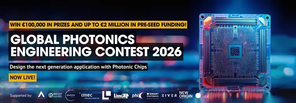
A good example of our involvement in this ecosystem is the Global Photonics Engineering Contest 2026. XIVER is one of the industrial partners supporting the initiative alongside other leading integrated photonics organizations. The contest is designed to help engineers, startups, researchers, and innovators develop new photonic chip applications, with access to technical support, industrial expertise, and potentially up to €2 million in investment. Our role reflects something we strongly believe in:
Great ideas need more than technical brilliance — they need a credible path to manufacturing and commercialization.
In fact, that's a theme we see across all our markets. Whether the customer is a startup or a multinational company, the challenge is usually not just creating breakthrough technology; it's achieving yield, reliability, scalability, and cost-effective production.
Ultimately, customers come to XIVER when they need help crossing the industrialization gap. We provide the process expertise, manufacturing know-how, and production infrastructure that enable advanced technologies to become successful products in the market.
Peter (PhotonDelta): At what stage do most companies first engage a manufacturing partner, and at what stage should they?
Sree (XIVER): In many cases, companies engage a manufacturing partner a bit later than they ideally should. Often, they first focus on proving that the technology works, building prototypes, and demonstrating performance. Only once they've achieved that milestone do they start thinking seriously about industrialization.
The challenge is that by then, some of the most important design decisions have already been locked in. The technology may work brilliantly, but it wasn't necessarily designed with manufacturing in mind.
We often see situations where a device performs exactly as intended in the lab, but when you try to scale it, yield becomes an issue; certain process steps prove difficult to reproduce consistently. At that point, redesigns can become expensive and time-consuming.
That's why we believe manufacturing should be part of the conversation much earlier. Ideally, we prefer that the customers involve us when they are still making key architecture and design decisions. That's the stage where small changes can have a huge impact on manufacturability, reliability, and ultimately time-to-market.
At XIVER, we always say that industrialization isn't something you do after innovation; it's something you build from the start. The earlier manufacturing expertise is brought in, the fewer surprises there are later.
This is particularly important in emerging fields like integrated photonics, where moving from a promising concept to a scalable product can be challenging. That's one of the reasons we're involved in initiatives like the Global Photonics Engineering Contest 2026: helping innovators think not only about what is technically possible but also about what can be successfully manufactured and commercialized.
In short, most companies engage a manufacturing partner after they've proven the technology. The most successful ones engage much earlier, when the design is still flexible, and manufacturing considerations can be built in from day one.
Peter (PhotonDelta): XIVER talks about concurrent engineering from day one. How does your approach differ from a traditional manufacturing partner?
Sree (XIVER): The traditional model is often quite sequential. A customer develops a technology, completes the design, proves the concept, and then hands it over to a manufacturer to figure out how to make it. By that point, many key decisions have already been made, and if manufacturing challenges emerge, the only option is often to go back and redesign.
At XIVER, we believe manufacturing expertise should be part of the development process from day one. That's what we mean by concurrent engineering. Instead of designing first and industrializing later, we work on both in parallel.
That means our process engineers, manufacturing specialists, and customer development teams are collaborating from the earliest stages. While the customer is optimizing performance, we're already thinking about process compatibility, yield, scalability, reliability, and cost. Those considerations influence design decisions long before the product reaches production.
A good example is when a customer develops a microsystem that performs exceptionally well in a laboratory environment. In a traditional hand-off model, the manufacturer might discover later that certain structures are difficult to produce consistently at scale, resulting in yield losses or process complexity. With concurrent engineering, those manufacturability questions are addressed upfront, so the design evolves with volume production in mind from the beginning.
Ultimately, we see ourselves as more than a foundry. We're a development and industrialization partner.
Peter (PhotonDelta): How does DfM look different for integrated photonics versus Micro-Electro-Mechanical Systems (MEMS) applications? Are there integrated photonics-specific constraints that engineers often underestimate?
Sree (XIVER): There are similarities between MEMS and integrated photonics when it comes to DfM. In both cases, success depends on translating a promising device concept into something that can be fabricated reproducibly. But the manufacturing sensitivities are often quite different.
Compared to MEMS, constraints in integrated photonics can be much less visible, which is why they're sometimes underestimated. Small process variations that are barely noticeable from a manufacturing perspective can have a significant impact on optical performance.
One misconception we occasionally encounter is that once the optical design has been simulated successfully, the manufacturing part will be straightforward. Photonic devices are often extremely sensitive to process variation. Designing for nominal performance is not enough, you also need to design for manufacturing tolerances.
Another area that's frequently underestimated is packaging and integration. In many photonic applications, the chip itself is only part of the challenge. Efficient optical coupling, alignment tolerances, thermal management, testing, and integration into a larger system can become just as important as the photonic circuit design itself.
We also see engineers focus heavily on device-level performance while underestimating questions such as scalability, testability, and production yield. A design that achieves record performance in a demonstration environment may not be the design that can be manufactured economically in larger volumes.
That's why at XIVER we try to bring manufacturability considerations into the discussion very early. We don't just consider whether a photonic device can be fabricated, we consider whether it can be fabricated repeatedly, with stable performance, acceptable yield, and a realistic path to production.
This is particularly relevant as integrated photonics moves into larger commercial markets such as high-speed data communications, sensing, AI infrastructure, and healthcare. The industry is increasingly shifting from proving what is technically possible to proving what can be produced reliably at scale.
Suggested reading: Transforming Sensing with Photonic Integrated Circuits
That's also one of the reasons we're involved in initiatives like the Global Photonics Engineering Contest 2026. Helping innovators think about manufacturability, integration, and scalability from the beginning is exactly where XIVER can add value.
In short, MEMS DfM is often about controlling mechanical structures and process robustness. Integrated photonics DfM is frequently about managing extremely tight optical tolerances, packaging, integration, and performance variation; areas that many teams underestimate until they start scaling toward production.
Peter (PhotonDelta): If you could give one piece of advice to teams participating in the Global Photonics Engineering Contest 2026, what would it be?
Sree (XIVER): Don't just ask yourself, 'Can I build it?' Ask yourself, 'Can I build it a thousand times, reliably and economically?'
Innovation doesn't end when the prototype works; it begins when you can manufacture it.
Key Takeaways for Integrated Photonics Innovators
- Technical performance is necessary, but not sufficient. A device that works in the lab must also work on the production line, repeatedly, reliably, and economically.
- Design for Manufacturing from day one. Photonic devices are highly sensitive to process variation.
- Engage manufacturing partners early. The most costly mistakes in photonics industrialization happen when design decisions are locked in before manufacturing expertise enters the conversation.
Ready to scale your photonic innovation? Learn how XIVER helps teams bridge the gap from prototype to production at xiver.com.