Wafer Probing: An Ultimate Guide
Wafer Probing is an electrical testing process conducted on semiconductor wafers after the integrated circuits are applied to the wafers. This is an essential step in the semiconductor manufacturing process that helps to determine the functionality of wafers and overall production quality. This article explores the process, importance, types, and applications of wafer probing.

27 Mar, 2023. 7 minutes read
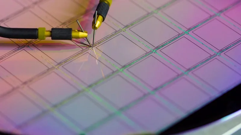
Checking Wafer Microchip with Probe Station
Introduction
Before silicon dies are assembled into packages, they undergo a wafer probing test process. The goal of this test is to identify ineffective wafers, providing valuable feedback that can significantly impact wafer fabrication, quality control, and production process control. This testing process requires the application of a piece of equipment called a wafer prober.
Wafer probing machines are automatic testing equipment used in the semiconductor manufacturing process to electrically test the integrated circuits of each wafer die. Two probes are used to measure and assess the electrical properties of the transistors, connections, and other circuit components as they move from one integrated circuit to the next.
Wafer Probing: Definition and Importance
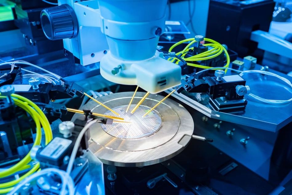
Wafer probing is a process in semiconductor development and manufacturing where each dies on a wafer is electrically tested. This is performed with an automated wafer probing system. The system holds a wafer on a stable mount and places a set of very thin pins on designated probe pads on the die. These probe pads are also called contact or connection pads, which the wafers connect to with the help of the precision point pins. The needles provide the electrical contacts needed to test the die properly. Bond pads are also used as probe pads.
The probe system is usually connected to a piece of automatic test equipment (ATE) which carries out the required electrical test on each die. The test equipment connected to the earlier mentioned pins provides the individual chips with a voltage, testing the correct functioning of each chip at the same time. Probing is done to ensure that the wafer has no defects that may result in low electrical yields after the wafer has been assembled into units, thereby saving costs for testing and assembly.
Wafer probing bears considerable significance in semiconductor and microelectronics manufacturing. Manual wafer probing is primarily used to assess the characteristics of prototype integrated circuits and evaluate defect signs. Additionally, it offers extremely accurate measurement and evaluation of a test element group (TEG) for an integrated circuit made up of transistors, connectors, and other components. To assess wafer dependability in both low and high temperatures, a wafer probe has a temperature control feature.
Automatic wafer probing is necessary for semiconductor mass production testing to ensure precise placement and high-speed controls during the TEG testing procedure. while inspecting the wafers of integrated circuits for flaws, the probe conducts a remove or proceed assessment. [1]
Wafer Probing Process
This is the application of the wafer probing system for the electrical testing of wafers on individual chips. A wafer probe loads and accurately positions the wafer, on a round plate called a wafer chuck. The wafers are subsequently moved into electrical contact with a collection of tiny needles called a probe card. The devices on a wafer receive test signals transmitted from this measuring instrument and send them back. In other words, test signals from the measuring instrument or tester are transmitted to individual devices on a wafer through the connected probe needles or a probe card and the signals are then returned from the device.
Some basic requirements for the wafer probing process are explained below:
Wafer Prober: used to handle the wafer by placing it on a chuck to be probed.
Probe Card: a tool that is fixed on a prober and connected to a tester.
Tester: used to process the data from the wafer probed and provide the probing results.
Wafer Map: a copy of the actual wafer, marked accordingly to indicate the pass and fail dies determined by the tester. This decides which dies are to be picked for the die attach process.
Preparation
In preparation for the test, the automatic test equipment (ATE) is made available, including the probe card, load board, wafer probe station, handler, DUT (Device Under Test) Board, etc.
Test Structure Design
Here, the design specifications and test specifications are provided in a datasheet to formulate the test plan and develop the test procedures. Probe structures must be designed with accuracy and their power delivery features must be optimized accordingly.
Alignment and Testing
A wafer prober aligns the bonding pad of a wafer with a needle in a probe card. This involves a wafer holder holding the wafer, and a photoelectric detector that detects the surface of the wafer to collect the alignment information needed to align the bonding pad with the probe pin in X and Y directions. After everything is determined to be properly aligned, the testing sequence can begin. [2]
Types of Wafer Probing
There are different types of wafer probing systems, discussed subsequently.
DC Probing
DC probing test involves checking for the presence of a short circuit or break in the circuit. This check encompasses the output current of the circuit as well as the input and output voltage. DC continuity testing determines that the pins of the chip and their connections are intact. It also includes checking that the DC electrical parameters are within a specific range.
RF Probing
RF probing is conducted on wafers for devices that work on radio frequencies such as RF transceivers, RF LNA, RF switches and Power Amplifier, and so on. It covers a wide range of applications based on WLAN, GSM, LTE, and Bluetooth standards. RF probing has been known to feature the following:
Delivering high first pass design, due to the probe tip included in the test setup calibration, resulting in accurate measurements.
Test results can be easily reproduced due to the automation of modern test probe alignment.
The correlation between the wafer and module test results is excellent with minimum variation.
Considerably short cycle time is required for production tests.
A completely automated test setup ensures a higher yield. This translates to lower test costs.
Parametric Probing
Parametric probing or wafer acceptance test (WAT), is carried out on the wafer after the metal has been laid on it, allowing probes to make electrical contact with special test structures. The test structures, which simulate actual devices as proxies, are designed to facilitate quick data collection and diagnose production processes. With this test, semiconductor manufacturers can ensure that the wafer production process is consistent and produces maximum yields from their substrates.
Parametric probing measures the electrical parameters of the device including Integrated Circuits, Resistors, Capacitors, Diodes, Transistors, and Inductors within specified limits. These tests provide historical data for decision-making by identifying the performance characteristics of the device being tested. The generated results are used to inform production, as new wafer process technologies can be developed and in-line and end-of-line processes can be monitored.
Wafer-Level Reliability Testing
Wafer Level Reliability (WLR) testing can be used to provide fast feedback process control information regarding what processes or mechanisms could cause premature IC failure and affect the reliability of a semiconductor device. This test serves to measure the variation in the materials that make up the semiconductor device and streamline new IC designs and process verification by evaluating the reliability features of the process.
By operating the device at its usable limits, reliability testing simulates the device's lifespan against recognized failure mechanisms. These tests are conducted on built-in structures in the wafer to collect data and ensure it can be done earlier in the manufacturing process. [3]
Wafer Probing Applications
This section covers the applications of wafer probing test systems in different levels of semiconductor fabrication.
Semiconductor Device Testing
Semiconductor test equipment such as IC tester is a system that will give electrical signals to the IC chips to compare its value. Then the value received by the system is compared with the expected value of the IC chips. This test determines whether the device is working as it was designed to. The most common IC testings are wafer testing and board-level testing. In most industries, wafer probing is conducted at the production level and before the installation of the chips onto the intended electronic device.
Failure Analysis
After fabricating the semiconductor wafer, every die on each wafer is subjected to probe testing to detect and isolate faults. Typical failure techniques used on the wafer include mechanical probing and electron beam probing. The tested wafers are diced and the good dies are packaged and tested further. A fraction of the tested wafers are selected to perform failure analysis. During failure analysis, a fraction of the defective die on the sampled wafers are carefully analyzed to detect the dominant cause of failures. Based on this analysis, corrective actions are taken on the piece of fabrication equipment found responsible for the observed failures.
Design Verification
Design verification techniques are similar to Failure Analysis. The goal is to verify whether the chip design was manufactured correctly since there can be imperfections in the fabrication process that may cause defects.
For this reason, the chips are screened through wafer probing, where the IC is fired-up by probe cards and the micro-probing is conducted via several single probes simultaneously. This is performed at the wafer level, whereas other verification tests such as burn-in test, structural test, characterization, and functional test are done at different levels of manufacturing. [4]
Key Takeaways
Wafer Probing is an electrical test that is conducted on semiconductor wafers with the help of a probe card. The probe card is placed onto a prober and connected to a tester, to establish an electrical path between the wafer and the tester. The probe card subsequently connects with the pads of the integrated circuit chips on the wafer using its metallic elements or needles to transmit the electrical data and necessary test parameters.
Wafer probe testing is used by semiconductor manufacturers to characterize the parts on the wafer, as the first of many steps. It is not intended to be the final test of the device after it has been packaged. Probe tests are used to identify and remove die that are unsuitable for packaging.
References
1. Any Silicon. Guide to Semiconductor Wafer Sort. 2023. [Cited 2023 Mar 24] Available from: https://anysilicon.com/guide-semiconductor-wafer-sort/
2. Rayming PCB & Assembly. Importance of a Probe Card PCB in Semiconductor Wafer Test System. 2021. [Cited 2023 Mar 24] Available from: https://www.raypcb.com/probe-card-pcb/
3. Any Silicon. What is a Probe Card? 2023.[Cited 2023 Mar 24] Available from: https://anysilicon.com/what-is-a-probe-card/
4. Wafer World. What is a Wafer Prober? 2021. [Cited 2023 Mar 25] Available from: https://www.waferworld.com/post/what-is-a-wafer-prober