New clock families for networking and computing applications
SiTime's FemtoClock 4 jitter attenuators fit up to 18 outputs in one BGA; the 12-output VersaClock 8 clock generator lists 10 fs maximum PCIe 7 jitter.

18 Nov, 2026. 4 minutes read
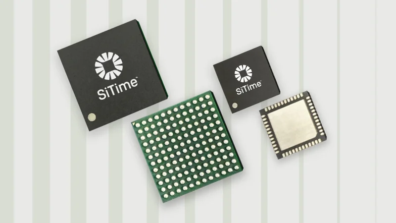
FemtoClock 4 and VersaClock 8
MEMS timing company SiTime has launched the FemtoClock 4 and VersaClock 8 clock families, both from the Renesas timing business it acquired in 2026.[1][2][3]
FemtoClock 4 is a jitter attenuator and clock generator for top-of-rack and spine switches built on 224G SerDes. SiTime claims 19 fs RMS jitter at 312.5 MHz in clock-generator mode (12 kHz to 20 MHz, 4 MHz high-pass filter) and up to six frequency domains across 18 outputs. VersaClock 8 is a programmable clock generator for CPU, xPU, memory and storage reference clocks, for which SiTime claims about 10 fs PCIe 7 jitter, 30 fs at 312.5 MHz under the same filter, and 105 °C operation. Both are in production.[1]
Clocks to address faster ethernet and connectivity standards
Ethernet specifies a 4 MHz clock-data-recovery bandwidth, so receivers track out slower reference jitter. Texas Instruments accordingly quotes the 224G budget through a 4 MHz high-pass filter: 35 fs RMS for a 312.5 MHz reference. PCIe 7.0 at 128 GT/s tightens the reference clock limit from PCIe 6.0's 100 fs to 67 fs.[4][5][6]
FemtoClock 4 jitter is comparable to competing parts. The Rev 1.00 FemtoClock 4 datasheets list 25 fs typical and 30 fs maximum at 312.5 MHz under that filter in synthesizer mode, above SiTime's 19 fs. TI's LMK5B33216 network synchronizer quotes 24 fs typical at the same frequency and filter, and Skyworks claims 17 fs for 224G SerDes from its SKY63101/02/03 jitter attenuators, filter unstated.[5][7][8][9][10]
The gain is density: FemtoClock 3 offered up to 12 outputs and four frequency domains in QFN packages; FemtoClock 4 puts 18 outputs in a 10 × 10 mm BGA.[8][9] The six independent time domains belong to the RC38616 radio synchronizer alone; the RC38412 has four and the RC32418/RC32412 switch parts two.[7][9][11] Boards using the 100-BGA parts of FemtoClock 3 Wireless, the radio-oriented FemtoClock 3 line, can take the 9 × 9 mm FemtoClock 4 versions: same body and crystal, two repurposed pins, changed supply-rail assignments, renumbered outputs and retuned crystal load settings.[12]
VersaClock 8 moves further on jitter. The 9- and 12-output VersaClock 8 parts list 10 fs maximum PCIe 7 jitter, 15% of the 67 fs limit (author's calculation); Diodes' six-output PI6CG33A06 PCIe 7 clock generator quotes under 30 fs.[13][14] Against its predecessor VersaClock 7, typical 12 kHz to 20 MHz jitter falls from 150 fs to 102 fs and the ambient rating rises from 85 °C to 105 °C, in the same 4, 5 and 6 mm square body sizes.[15][16][17] VersaClock 7 B-revision parts already list PCIe 7 readiness, so moving from them buys those gains, not PCIe 7 support.[16]
Technical specifications
FemtoClock 4 (RC38616, RC38412, RC32418, RC32412)
| Spec | RC38616 / RC32418 | RC38412 / RC32412 |
|---|---|---|
| Differential outputs | 18 | 12 |
| Package | 10 × 10 mm 144-BGA | 9 × 9 mm 100-BGA |
| Independent timing domains | 6 (RC38616), 2 (RC32418) | 4 (RC38412), 2 (RC32412) |
| Phase jitter, 312.5 MHz, 12 kHz to 20 MHz, 4 MHz HPF, synthesizer mode (A2xx VCO option) | 25 fs typ, 30 fs max | 25 fs typ, 30 fs max |
| Phase jitter, 390.625 MHz, same filter, synthesizer mode | 22 fs typ, 25 fs max | 22 fs typ, 25 fs max |
| Phase jitter, 312.5 MHz, 12 kHz to 20 MHz, no filter, APLL steered by DPLL | 45 fs typ, 55 fs max | 45 fs typ, 55 fs max |
| Output frequency | CML to 2.5 GHz, LVDS/HCSL to 1 GHz, LVCMOS to 250 MHz | Same |
| Supply | 1.8 V | 1.8 V |
| Temperature | -40 to +85 °C ambient; -40 to +105 °C board | Same |
| DPLL compliance | ITU-T G.8262 and G.8262.1 | Same |
| Total power | Not stated (per-rail currents only) | Not stated (per-rail currents only) |
Sources: [7][9][11]
VersaClock 8 (RC31312A, RC31309A)
| Spec | RC31312A | RC31309A |
|---|---|---|
| Differential outputs | 12 | 9 |
| Package | 6 × 6 mm 48-QFN | 5 × 5 mm 40-QFN |
| PCIe 7 common-clock jitter | 4.2 fs typ (product page), 10 fs max | 4.2 fs typ (product page), 10 fs max |
| Phase jitter, 156.25 MHz, 12 kHz to 20 MHz | 102 fs typ | 102 fs typ |
| Output frequency | LP-HCSL 8 kHz to 650 MHz, LVCMOS 8 kHz to 200 MHz | Same |
| Supply | 1.8, 2.5 or 3.3 V | Same |
| Ambient temperature | -40 to +105 °C | Same |
| On-chip OTP | Up to 18 configurations | Same |
| Internal-crystal option | Yes (Q variant) | Yes (Q variant) |
Sources: [13][15][17][18][19]
The FemtoClock 4 jitter figures assume every output runs the same frequency from the analog PLL (APLL) through integer dividers. Fractional output dividers are noisier: 69 fs typical at 312.5 MHz unfiltered on the RC32418, against 45 fs from the APLL, so the headline numbers apply to the APLL domain only.[7] For synthesizer-mode designs at 156.25, 312.5 and 625 MHz, Renesas recommends a 62.5 MHz crystal to keep divider ratios integer.[20] The FemtoClock 4 datasheets give per-rail currents and refer power calculations to Renesas' RICBox software rather than stating a total, the main gap before design-in; the divider penalty only limits where the cleanest clocks come from.[7][9] The 5-output VersaClock 8 RC31305A comes in a 4 × 4 mm 32-pin QFN.[17]
Recommended reading
Phase Locked Loop (PLL): How It Works and How to Design One. Explains how loop bandwidth shapes reference and VCO noise and why fractional-N synthesis costs jitter, the mechanisms behind the APLL and divider figures above.
References
- SiTime Addresses $2 Billion Opportunity in Data Center Bandwidth Upgrades with Two New Clock Families, SiTime, 17 November 2026
- SiTime to Acquire Renesas' Timing Business, SiTime, 4 February 2026
- SiTime Clocks & Timing, SiTime, product portfolio page, accessed 18 November 2026
- Why It's Time to Rethink Jitter Analysis of SerDes Reference Clocks in Optical Modules, SiTime, 16 April 2025, technical blog on refclk jitter filtering
- 112G and 224G PAM4 SerDes Clocking for Rapid Data Center Switches (SNAA396A), Texas Instruments, January 2025, application note
- Verifying the true jitter performance of clocks in PCI Express and high-speed Ethernet designs, Rohde & Schwarz, undated, test-equipment application note
- RC32418/RC32412 Datasheet, Rev 1.00, Renesas, 2 October 2026
- Renesas' New FemtoClock 3 Timing Solution Delivers Industry's Lowest Power and Leading Jitter Performance of 25fs-rms, Renesas, 18 April 2024
- RC38616/RC38412 Datasheet, Rev 1.00, Renesas, 2 October 2026
- Skyworks Introduces New Programmable Bulk Acoustic Wave Clocks for 5G, 6G, and Data Center Applications, Skyworks, 6 November 2025
- RC38412 FemtoClock 4 Wireless 4-Channel Ultra-Low Phase Noise Synchronizer and Jitter Attenuator with 12 Outputs, Renesas, product page, accessed 18 November 2026
- FC3W 100BGA Device Upgrade to FC4 100BGA Device, Renesas, 23 October 2026, application note
- RC313xx Short-Form Datasheet, Rev 1.00, Renesas, 29 July 2026
- PCIe 7.0 Clock Generator from Diodes Incorporated Delivers Sub-30fs Jitter for Next-Gen AI Infrastructure, Diodes Incorporated, 6 May 2026
- RC313 VersaClock 8 Programmable Clock Synthesizer/Jitter Attenuator, Renesas, product page with VersaClock 7 comparison table, accessed 18 November 2026
- RC310 VersaClock 7 Programmable Jitter Attenuator Family, Renesas, product page, accessed 18 November 2026
- RC31312A-EVK VersaClock 8 Evaluation Kit Manual, Renesas, 30 July 2026
- RC31312A000GNA#BB0 VersaClock 8 Programmable Clock Synthesizer/Jitter Attenuator, Renesas, part page, accessed 18 November 2026
- RC31309A001GND#BB0 VersaClock 8 Programmable Clock Synthesizer/Jitter Attenuator, Renesas, part page, accessed 18 November 2026
- Choosing the Correct Crystal or XO for FemtoClock 4 and FemtoClock 4 Wireless, Renesas, 2 November 2026, application note