Schematic Symbols: Building Blocks of PCB Design
Every electronic design begins with abstraction.

12 Aug, 2026. 5 minutes read
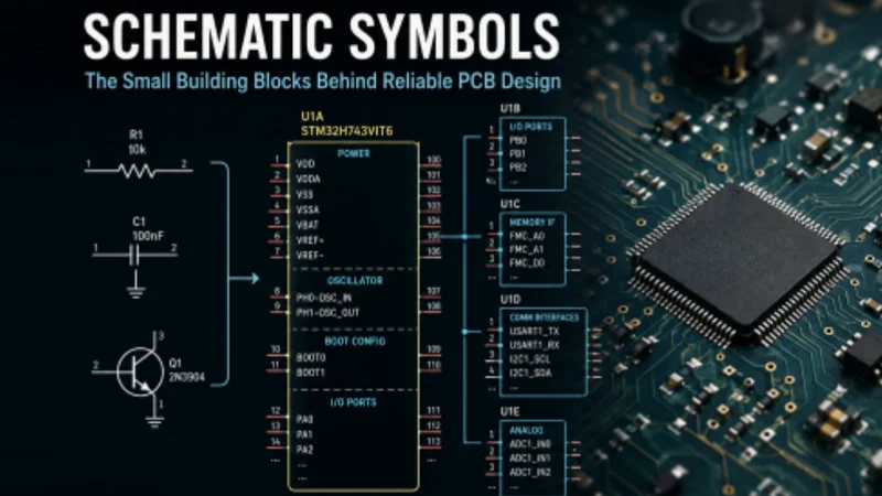
Before a component becomes a footprint on a PCB, before copper is routed and before a board is manufactured, it usually appears in the engineer’s design as something far simpler: a schematic symbol.
A resistor becomes a handful of lines. A transistor becomes three pins and a familiar shape. A complex microcontroller containing millions of transistors may be reduced to a collection of rectangles and labelled connections.
That simplicity is useful. It is also deceptive.
A schematic symbol is not merely an illustration of a component. It is a structured representation of how that component interacts electrically with the rest of a design. Pin numbers, pin names, electrical types, grouping and mapping all need to be correct. Errors introduced here can propagate through the entire PCB design process.
As components become more complex, creating and maintaining reliable schematic symbols becomes an increasingly important part of electronic design automation.
What Are Schematic Symbols?
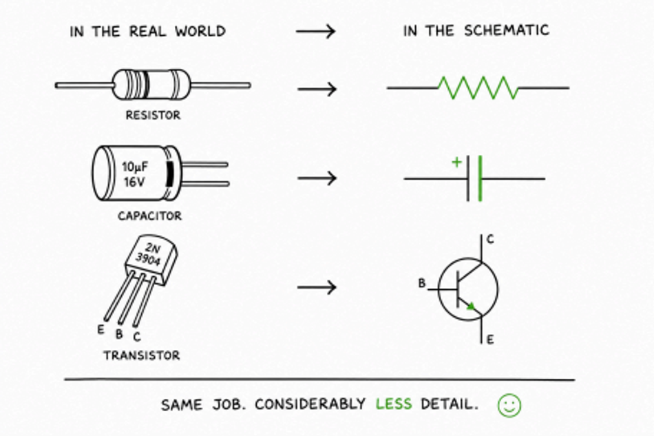
Schematic symbols are graphical representations of electronic components used within circuit schematics.
Rather than showing the physical appearance of a component, the symbol communicates its electrical function and connections. An engineer designing a circuit can therefore work with an understandable logical representation rather than the physical geometry that will eventually appear on the PCB.
A simple component might require only two or three pins. More sophisticated devices can contain hundreds or even thousands of connections.
The schematic symbol therefore sits at an important boundary between two worlds: the functional intent of the engineer and the physical component that will ultimately be placed onto a PCB.
For that reason, the information associated with the symbol matters at least as much as its appearance.
Symbol Creation Standards
Consistency is one of the foundations of a useful component library.
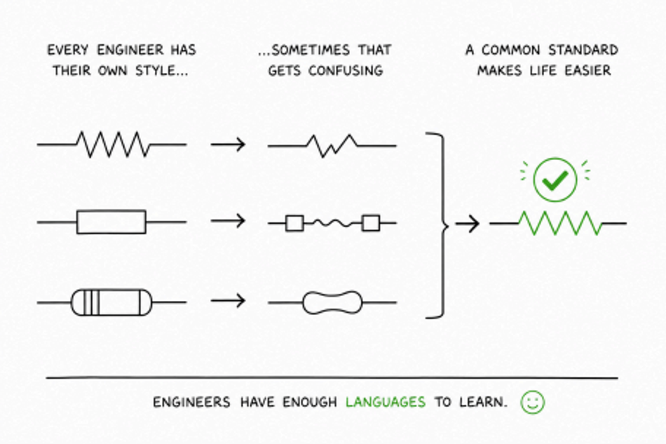
Standards such as IEC 60617 and IEEE/ANSI conventions provide recognised graphical approaches for many common electronic symbols. EDA tools and individual organisations may also have their own conventions governing symbol dimensions, pin spacing, orientation, naming and graphical presentation.
The objective is not simply to make a library look tidy.
Consistent electronic symbols make designs easier to read, review and maintain. Engineers should be able to understand the intent of a circuit without first learning the individual drawing habits of whoever created each component.
This becomes particularly important within larger organisations where libraries may be used across multiple engineering teams, locations and projects over many years.
A well-managed library effectively creates a common design language.
The Challenge of Multi-Part Components
Modern electronic components quickly expose the limitations of treating a schematic symbol as a simple drawing.
Consider a large FPGA, processor or other high-pin-count device.
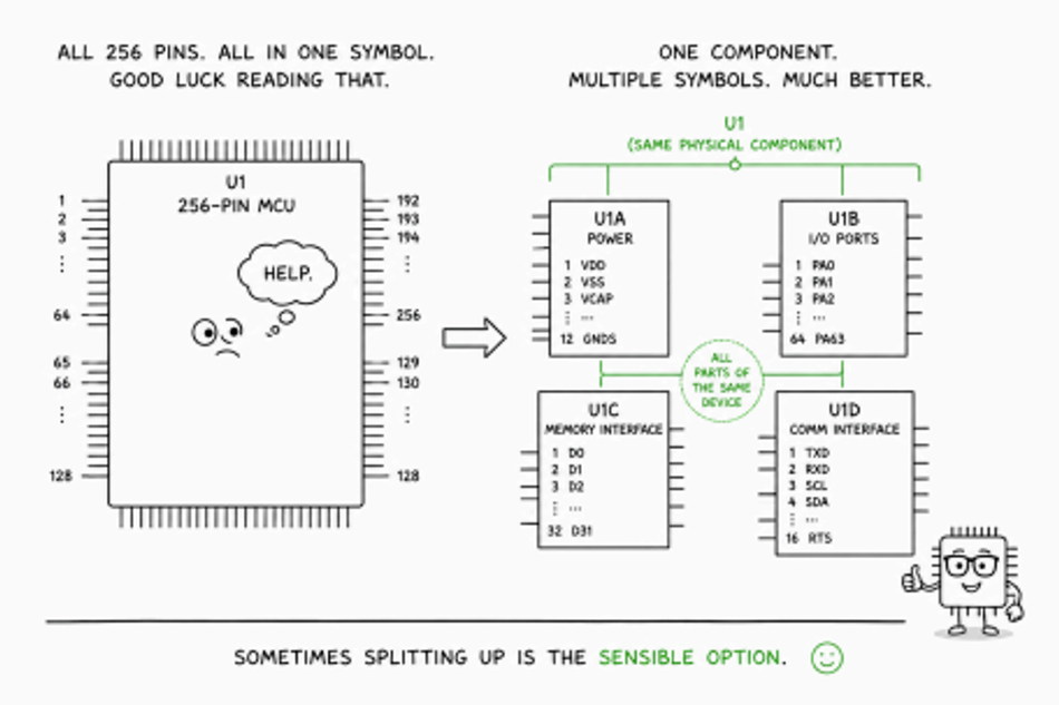
Displaying hundreds or thousands of pins inside a single symbol can make a schematic almost impossible to navigate. Components are therefore frequently divided into multiple logical sections or gates.
One section might contain power connections, another memory interfaces, another general-purpose I/O and another communications interfaces.
This makes the schematic substantially easier for an engineer to understand, but it also introduces another layer of complexity into symbol creation.
Every section still represents the same physical component. Pin numbering must remain unique and accurate, and every logical connection must eventually map to the correct physical pad within the PCB footprint.
The symbol has become a structured data model rather than simply a graphical object.
Pin Mapping: Where Small Errors Become Expensive
Pin mapping is one of the most important elements of component library creation.
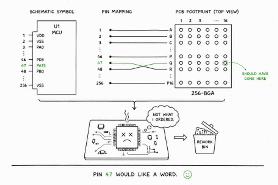
Each schematic pin must correspond correctly with the physical pad defined within the PCB footprint.
For a two-pin resistor this is straightforward.
For a 500-pin BGA, the problem is very different.
Pin names and numbers need to be interpreted from manufacturer documentation and translated accurately into the EDA library. Power pins, grounds, differential pairs, no-connect pins and specialised functions all need to be represented correctly.
A single incorrect mapping can potentially result in a PCB that passes through schematic capture and layout before the problem is discovered during design review, prototyping or even manufacture.
At that point, what began as a tiny library-data error can become a costly engineering problem.
This is why component libraries should increasingly be considered part of the engineering data infrastructure rather than collections of drawings.
Library Management Best Practices
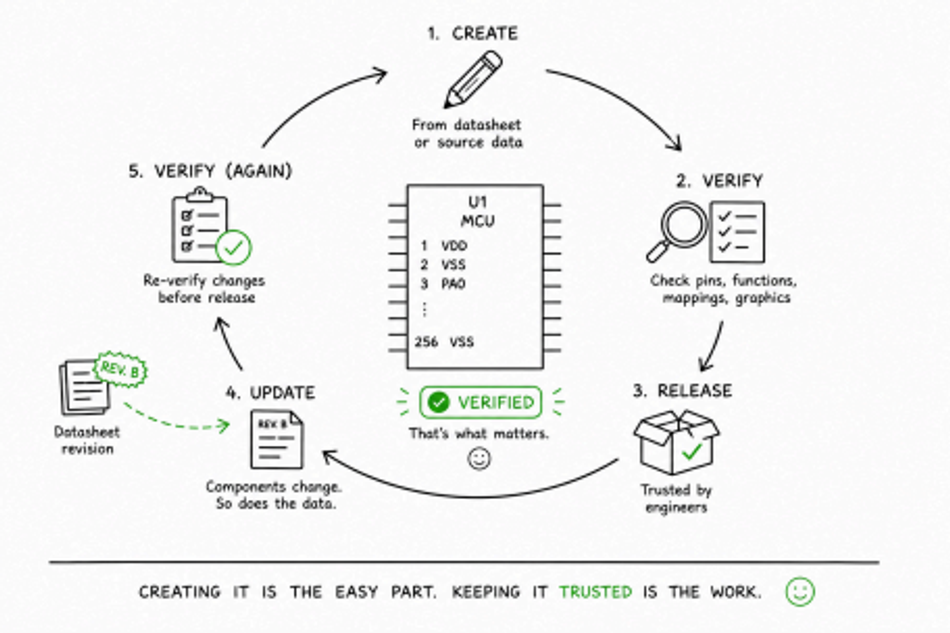
Creating a good schematic symbol is only the beginning.
Components change. Manufacturers revise documentation. New packages appear. Errors are discovered. Engineering teams introduce new requirements.
The real challenge is maintaining trusted component data over time.
Good library management therefore needs processes for creation, validation, version control, change management and feedback.
It should also be clear where component information originated and how it has been verified.
For engineering organisations maintaining their own libraries, this can become a substantial ongoing workload. The larger the component library becomes, the greater the challenge of keeping everything consistent and current.
There is also an important distinction between having a component library and trusting one.
Engineers will often spend time checking a downloaded model against a manufacturer datasheet because the cost of discovering an error later in the design process is significantly greater than the time spent validating it upfront.
Trust is therefore one of the most valuable characteristics any component library can provide.
Automated Symbol Generation
Automation has the potential to change this process significantly.
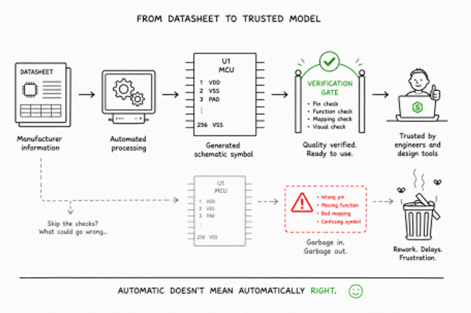
Many of the attributes required to construct schematic symbols already exist somewhere within component documentation or structured manufacturer data.
Pin numbers, pin names, electrical functions and package information can increasingly be extracted, interpreted and transformed into EDA-ready component models.
Automation can accelerate creation, improve consistency and make it practical to support a much larger universe of electronic components.
But automation alone does not solve the problem.
Generating a symbol quickly is valuable only if the resulting data is correct.
The real opportunity is therefore to combine automation with validation, structured data management and feedback systems capable of improving models over time.
As AI becomes more capable of interpreting technical documentation, the boundary between manually created and automatically generated engineering content is likely to move considerably.
The question may eventually shift from “Can this component model be generated automatically?” to “How do we prove that the automatically generated model can be trusted?”
That is a much more interesting engineering problem.
From Schematic Symbols to a Digital Component
Schematic symbols are only one representation of an electronic component.
The same component may also require a PCB footprint, 3D model, simulation data, technical specifications, lifecycle information, pricing, availability and manufacturer documentation.
Historically, many of these data types have existed separately.
Increasingly, they are becoming connected.
The longer-term opportunity is to move beyond individual files towards a trusted digital representation of a component that can flow through the engineering process.
For engineers, that means spending less time searching for, creating and checking component data and more time actually designing.
A schematic symbol may look like one of the simplest objects in an electronic design.
But behind those few lines and pins sits a surprisingly complex data problem - and solving that problem well is fundamental to reliable PCB schematic design.
Alex MacDougall is the founder of SamacSys and author of Built, Not Given, a forthcoming book about building a global engineering technology business from nothing—and the setbacks, decisions and lessons that shaped the journey.
Learn more about Built, Not Given at: AlexMacDougall.com