PCB Footprints: A Comprehensive Guide to Land Pattern Design
Master the essentials of PCB footprint design with practical guidance on land patterns, industry standards, common pitfalls, and proven verification techniques to improve manufacturability, reduce assembly defects, and ensure reliable, production-ready circuit boards.

08 Jul, 2026. 5 minutes read

Every PCB design lives or dies by its details, and few details matter more than the footprint. Get a PCB footprint wrong and you're looking at tombstoned components, cold solder joints, or a board that simply doesn't fit its enclosure. Get it right and assembly runs smoothly, yields stay high, and rework stays rare. This guide walks through what a footprint actually is, the standards that govern land pattern design, the mistakes that trip up even experienced designers, and how to build and verify footprints you can trust.
What Is a PCB Footprint?
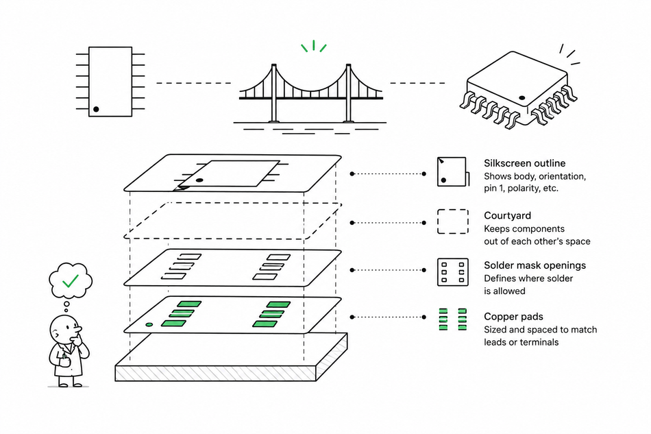
A PCB footprint - also called a land pattern - is the arrangement of copper pads, silkscreen markings, solder mask openings, and mechanical outlines that define where and how a component physically attaches to a board. It's the bridge between a schematic symbol (an electrical abstraction) and the real, physical part that gets placed and soldered.
A complete footprint typically includes:
Copper pads - sized and spaced to match the component's leads or terminals
Solder mask and paste layers - that control where solder flows during reflow
Silkscreen outline - showing the component's body and orientation (pin 1 marker, polarity, etc.)
Courtyard - boundaries that prevent placement conflicts with neighboring parts
Because the footprint determines whether a physical part can actually be soldered down correctly, it's one of the highest-leverage - and highest-risk - elements in the entire circuit board design.
IPC Footprint Standards.
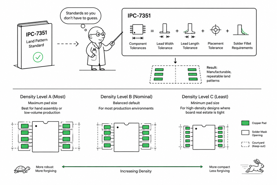
Most professionally designed footprints follow IPC-7351, the industry standard for surface-mount land pattern design. IPC-7351 defines pad sizing based on manufacturing tolerance classes:
Density Level A (Most) - maximum pad size, best for hand assembly or low-volume production
Density Level B (Nominal) - balanced default for most production environments
Density Level C (Least) - minimum pad size, used for high-density designs where board real estate is tight
The standard calculates land pattern dimensions from the component's physical tolerances, not just its nominal size - accounting for lead width, lead length, placement tolerance, and solder fillet requirements. Following IPC-7351 (or its through-hole counterpart, IPC-2221, alongside connector- and package-specific standards) gives designers a repeatable, manufacturable baseline rather than reinventing pad geometry for every part.
Common Footprint Mistakes
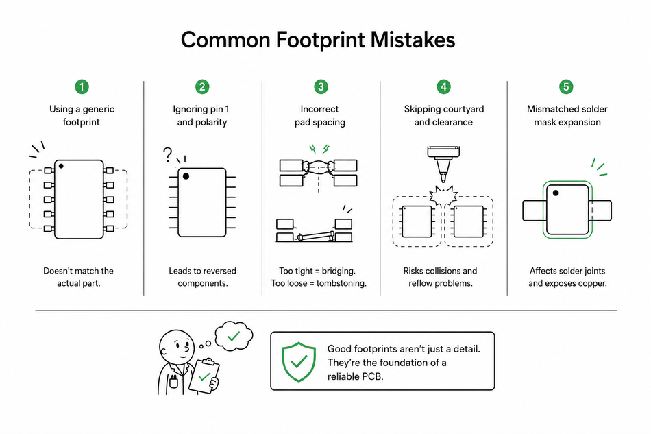
Even with standards available, footprint errors are among the most frequent causes of PCB assembly failures. A few stand out.
Using a generic footprint instead of the exact part dimensions.
It's tempting to grab a "standard" 0805 or SOIC-8 footprint from a library and assume it fits. But body size, lead pitch, and lead length vary between manufacturers - sometimes significantly - even within the same nominal package. A generic footprint built around an assumed body size, rather than the datasheet dimensions of the specific part you're using, can leave pads too short, too long, or misaligned with the actual leads. Always start from the manufacturer's mechanical drawing for the exact part, not a family-average footprint.
Ignoring pin 1 orientation and polarity markings.
Missing or ambiguous polarity indicators are a leading cause of reversed components during assembly.
Incorrect pad-to-pad spacing.
Pads that are too tight invite solder bridging; pads that are too generous can cause tombstoning on small passives during reflow.
Skipping courtyard and clearance checks.
Without proper courtyard boundaries, footprints placed too close together can cause placement machine collisions or thermal issues during reflow.
Mismatched solder mask expansion.
Incorrect mask openings can leave copper exposed where it shouldn't be, or mask off area needed for a proper solder joint.
Creating Custom Footprints
When a part doesn't have a library footprint available, custom creation is necessary - and it should always start with the datasheet, not a similar-looking existing part. Key steps:
Pull exact mechanical dimensions from the manufacturer's datasheet (body size, lead pitch, lead width, lead length, and tolerances).
Calculate pad geometry using IPC-7351 formulas or a trusted calculator tool, selecting the appropriate density level for your assembly process.
Build the courtyard, silkscreen outline, and pin 1 marker to match the physical part.
Add or verify a 3D model that matches the actual component body height and shape.
Cross-check the finished footprint against the datasheet's recommended land pattern, if the manufacturer provides one.
Skipping the datasheet step and eyeballing dimensions from a picture or a similar part is one of the most common ways custom footprints go wrong.
Verifying Footprints Before Manufacturing
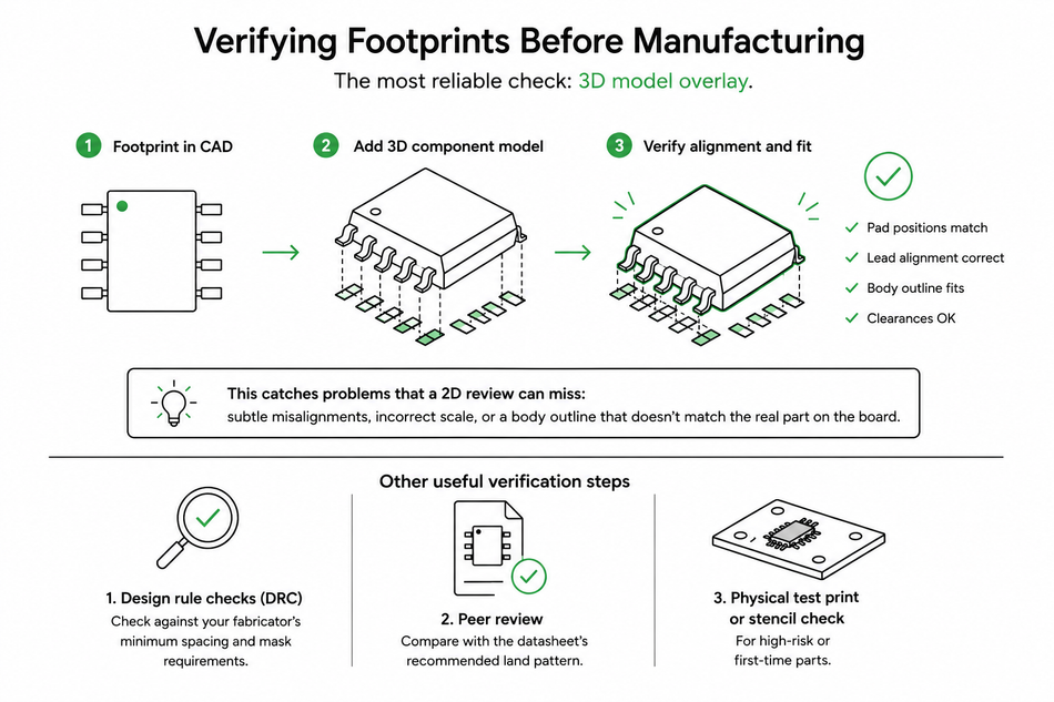
No footprint should go to fabrication without verification. The most reliable check is a 3D model overlay: placing the component's 3D mechanical model directly onto the footprint in your CAD tool to visually confirm that pad positions, spacing, and outline genuinely match the physical part. This catches problems that a 2D land pattern review can miss entirely - subtle lead misalignments, incorrect scale, or a body outline that doesn't match the real footprint of the part on the board.
Other useful verification steps include:
Design rule checks (DRC) against your fabricator's minimum spacing and mask requirements
Peer review against the datasheet's recommended land pattern
A physical test print or stencil check for high-risk or first-time parts
Automated Footprint Generation
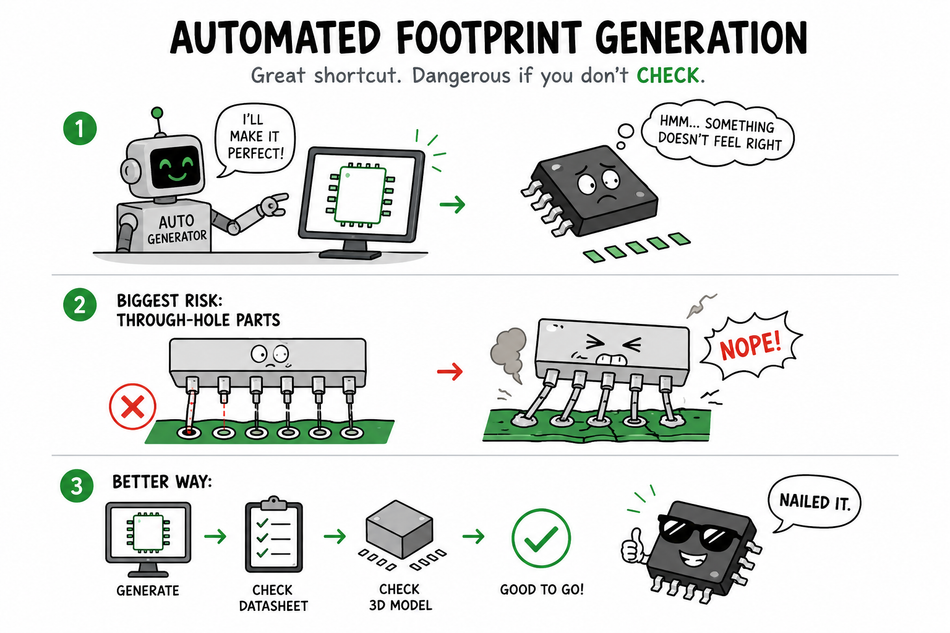
Automated footprint generators can save significant time, but they carry real risk if used carelessly. A generator that isn't tied back to verified physical dimensions - or that hasn't been checked against an accurate 3D model - can produce a footprint that "looks right" but doesn't actually match the part.
The most common failure mode is with through-hole components: automated tools can generate hole sizes or positions that don't correctly line up with the component's actual pins, especially for connectors or parts with non-standard hole patterns. A footprint can pass a visual check and still fail on the assembly line if hole diameter, position, or plating clearance is off by even a fraction of a millimeter.
The safest approach treats automation as a starting point, not a final answer: generate the footprint, then verify it against the manufacturer's mechanical drawing and a 3D model before it ever reaches a bill of materials or a production file.
Getting Footprints Right the First Time
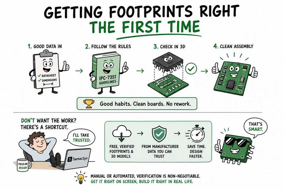
Footprint accuracy is ultimately a data problem - the quality of your land pattern is only as good as the dimensional data behind it. Building footprints from verified datasheets, following IPC-7351 guidelines, and confirming fit with a 3D model overlay before release are the habits that separate boards that assemble cleanly from boards that end up in the rework pile. Whether you're building footprints by hand or leaning on automated tools, that verification step is non-negotiable.
If you’d rather skip the manual creation and verification work entirely, services like SamacSys offers free, verified footprints and 3D models sourced directly from manufacturer data - letting you pull a trusted land pattern straight into your design instead of building and checking one from scratch. Of course, this choice of personal creation vs a service provider is something you and your organisation will have to consider and weight up on a case-by-case basis.
Alex MacDougall is the founder of SamacSys and author of Built, Not Given, a forthcoming book about building a global engineering technology business from nothing—and the setbacks, decisions and lessons that shaped the journey.
Learn more about Built, Not Given at: AlexMacDougall.com