PCB Component Placement: Rules, Techniques & Best Practices
Discover the fundamentals of PCB component placement, from optimising signal integrity and thermal performance to minimising EMI and avoiding common layout mistakes that can compromise manufacturability and reliability.

20 Nov, 2026. 6 minutes read
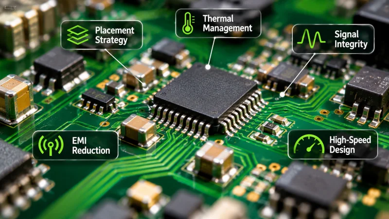
There’s a point in almost every PCB design where everything looks perfectly reasonable on the schematic, and then you open the layout and realise you’ve somehow got to fit it all onto a board roughly the size of a digestive biscuit.
Welcome to PCB component placement.
It’s one of those stages of electronic design that looks deceptively simple. You’ve got your components, you’ve got your board outline, and you’ve got a mouse. How difficult can it be?
Quite difficult, as it turns out.
Poor component placement can introduce signal integrity problems, thermal hotspots, electromagnetic interference (EMI) and manufacturing headaches before you’ve even routed the first track.
And while modern PCB design software has become remarkably sophisticated, it still can’t compensate for every questionable decision made by the person operating it.
The good news is that effective PCB component placement isn’t magic. It’s about understanding a few fundamental principles, making sensible compromises and, ideally, avoiding the sort of mistakes that only become obvious after you’ve ordered 500 boards.
1. Placement Strategy: Start With the Components That Have No Choice
One of the most useful PCB component placement guidelines is to start with the components whose positions are dictated by the product itself.
Connectors need to line up with enclosures. Mounting holes need to match mechanical fixings. Buttons and LEDs generally need to be somewhere a human can actually reach or see them.
There’s little point spending an afternoon creating a beautiful layout only to discover that the USB connector is pointing directly into the side of the enclosure.
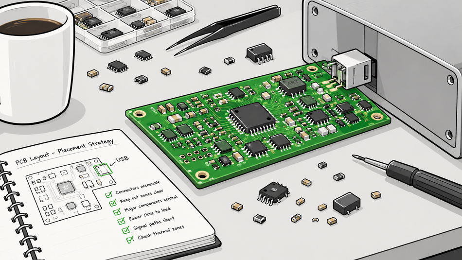
Once the mechanically constrained components are positioned, arrange the major functional blocks: power supplies, processors, memory, analogue circuitry and communication interfaces.
Think about how signals and power move between these blocks. Components that communicate frequently should generally be positioned to allow short, direct connections, while sensitive circuitry may need separation from electrically noisy areas.
Don’t confuse proximity with good placement, though. Sometimes putting components further apart is exactly the right decision.
And leave enough room for routing, testing and assembly. A board that looks wonderfully compact before routing can become considerably less impressive once you try connecting everything together.
The objective isn’t to fit everything into the smallest possible space. It’s to create a layout that works electrically, mechanically and practically.
2. Thermal Considerations: Heat Has to Go Somewhere
Electronic components generate heat. Some generate considerably more than others, and pretending otherwise rarely ends well.
Power regulators, MOSFETs, processors and high-current components deserve particular attention during placement.
Putting several heat-generating components close together might make the functional blocks look tidy, but it can create a concentrated hotspot that becomes difficult to manage.
Consider the available copper area, thermal vias, airflow, nearby temperature-sensitive components and the eventual enclosure.
A component’s temperature doesn’t depend solely on its own power dissipation. Its neighbours, the PCB construction and the surrounding environment all contribute.
Sometimes placing a heat-generating component closer to a suitable copper area or thermal path is more useful than simply moving it away from everything else.
And remember, a design that behaves perfectly on an open laboratory bench might become considerably less enthusiastic once it’s sealed inside a plastic box.
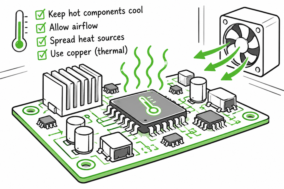
Good thermal management starts with component placement, not when somebody notices the enclosure is getting rather warm.
3. Signal Integrity: Shorter Isn’t Always the Whole Answer
Signal integrity is one of those subjects that becomes increasingly important as switching speeds and signal frequencies rise.
Long traces, poor return paths, impedance discontinuities and unwanted coupling can all affect how reliably signals travel across a PCB.
Component placement has a significant influence on these problems.
Position related devices to support short, direct signal paths, particularly where timing or impedance matters. Decoupling capacitors should be placed close to the relevant power pins, with low-inductance connections to power and ground.
But simply making every trace as short as possible isn’t a complete design strategy.
A slightly longer trace with a continuous reference plane and controlled impedance may perform considerably better than a shorter one that crosses a split in its return path.
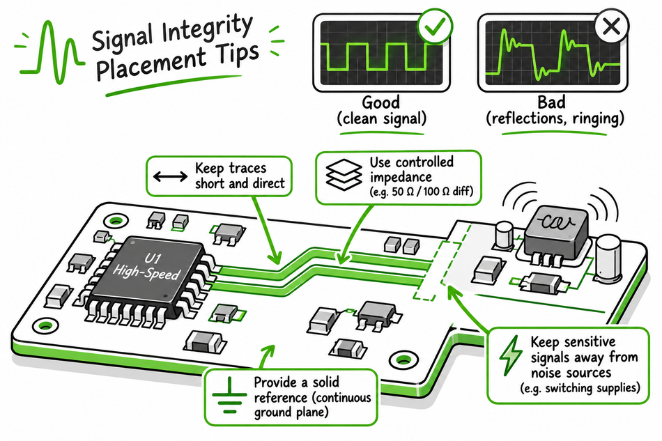
It’s also worth thinking about the relationship between analogue and digital circuitry. Sensitive analogue signals generally benefit from being kept away from noisy switching nodes and high-current paths.
The important thing is understanding where currents flow, including the return currents that aren’t always obvious from looking at the schematic.
A PCB doesn’t care how tidy your layout looks. It cares about the electrical paths you’ve actually created.
4. EMI Reduction: Don’t Create Problems You Then Have to Fix
Electromagnetic interference is another area where sensible component placement can save considerable trouble later.
Fast switching edges, high-current loops and poorly managed return paths can create unwanted electromagnetic emissions or make circuits more susceptible to interference.
Switching regulators are a good example.
Keeping the critical high-di/dt current loops compact is essential. Positioning the relevant capacitors, switching devices and associated components correctly can significantly reduce the loop area responsible for unwanted emissions.
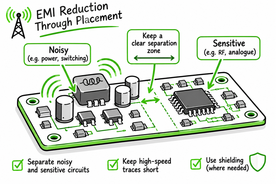
It’s also worth considering the position of connectors and cables, which can provide convenient paths for interference to enter or leave the board.
Keep noisy circuits away from sensitive inputs where practical, maintain appropriate reference planes and avoid routing critical signals through areas with poorly controlled return paths.
Grounding deserves particular care. Simply separating everything into different ground regions isn’t automatically an improvement, particularly if it forces return currents to take longer or less predictable routes.
I’ve always thought there’s something slightly frustrating about spending time fixing an interference problem that could have been avoided by moving a few components before routing.
Unfortunately, the laws of electromagnetism aren’t particularly interested in how much time you’ve already spent on the design.
5. High-Speed Design: Placement Becomes Part of the Circuit
In high-speed PCB design, component placement isn’t just about convenience. It becomes part of the electrical design itself.
Interfaces such as USB, Ethernet, DDR memory and other high-speed connections introduce additional constraints involving impedance, timing, skew, reference planes and signal coupling.
The exact requirements depend on the interface, but the underlying principle is consistent: placement decisions influence how easily those requirements can be met.
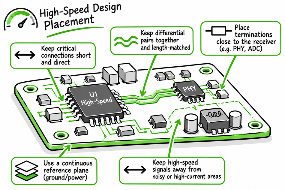
For example, positioning a processor and its associated memory without considering the routing topology can create unnecessary difficulties when matching signal lengths or maintaining suitable signal paths.
Differential pairs need appropriate routing geometry and consistent reference conditions. Placing connected devices sensibly makes these requirements much easier to achieve.
High-speed components also need suitable power distribution and decoupling arrangements, which should be considered during placement rather than squeezed into whatever space remains afterwards.
The temptation is to treat these as routing problems.
But by the time routing begins, many of the important decisions have already been made.
Good high-speed routing starts with good component placement.
6. Don’t Forget the People Who Have to Build It
It’s surprisingly easy to become so focused on electrical performance that manufacturability becomes an afterthought.
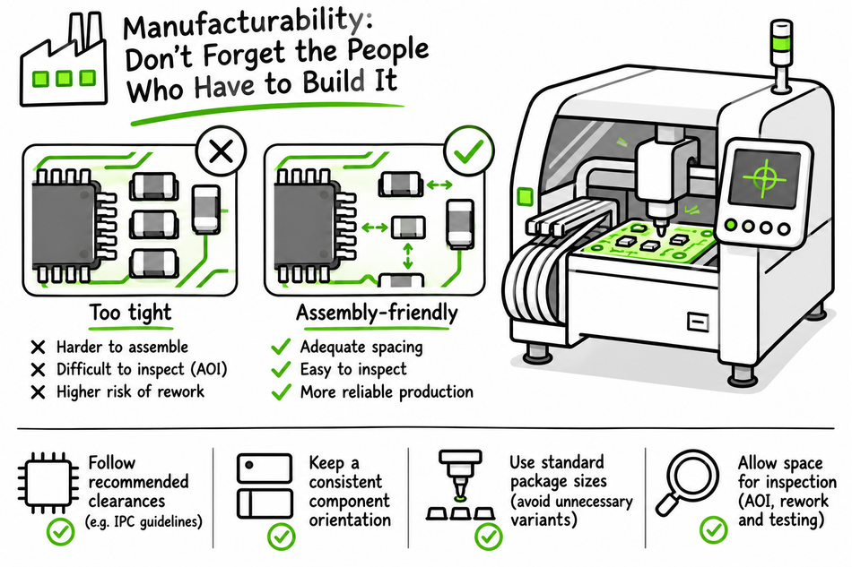
Component spacing, orientation, access for inspection, soldering requirements and assembly processes all influence whether a board can be manufactured reliably.
For example, placing components too close together can create difficulties with automated assembly, rework or inspection.
Test points also need consideration. There’s little benefit in providing a perfectly positioned test point electrically if nobody can physically reach it with a probe.
Accurate PCB footprints and component models matter here too.
A placement strategy is only as reliable as the component data behind it. Incorrect pad dimensions, component outlines or orientation information can undermine an otherwise perfectly reasonable design.
Having spent much of my career working on electronic component CAD models and the systems used to generate them, I’ve seen how important it is to get that underlying information right.
It’s not the most glamorous part of electronics engineering, but discovering that a component doesn’t physically fit after the boards have been manufactured is a fairly effective reminder of its importance.
Final Thoughts: Good Placement Makes Everything Else Easier
There’s no single perfect component placement strategy for every PCB.
A compact consumer product, a high-power industrial controller and a high-speed communications board will all have different priorities.
The skill lies in understanding those priorities and making informed compromises.
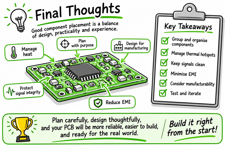
Start with the mechanical constraints, organise functional blocks logically, consider thermal behaviour, protect signal integrity, minimise EMI risks and keep manufacturability in mind.
Most importantly, don’t treat component placement as something to rush through before the supposedly interesting part of routing begins.
A few extra minutes spent getting placement right can save hours of routing, debugging and redesign later.
And if nothing else, try to make sure the connectors are pointing in the right direction.
It’s surprisingly helpful.