Model incorporates anisotropic conductivity to improve thin film devices
The new framework replaces approximations, accurately modeling current crowding and spreading resistance in 2D materials to improve high-performance semiconductor devices.
19 Mar, 2026. 4 minutes read
This article was first published on
news.engin.umich.eduThe high-performance semiconductor devices powering smartphone displays, AI computing, EV batteries and more are increasingly incorporating 2D materials to overcome silicon’s scaling limits. To optimize these technologies, a University of Michigan Engineering team developed a precise mathematical framework that accounts for anisotropic—or unevenly spreading—conductivity and device geometry.
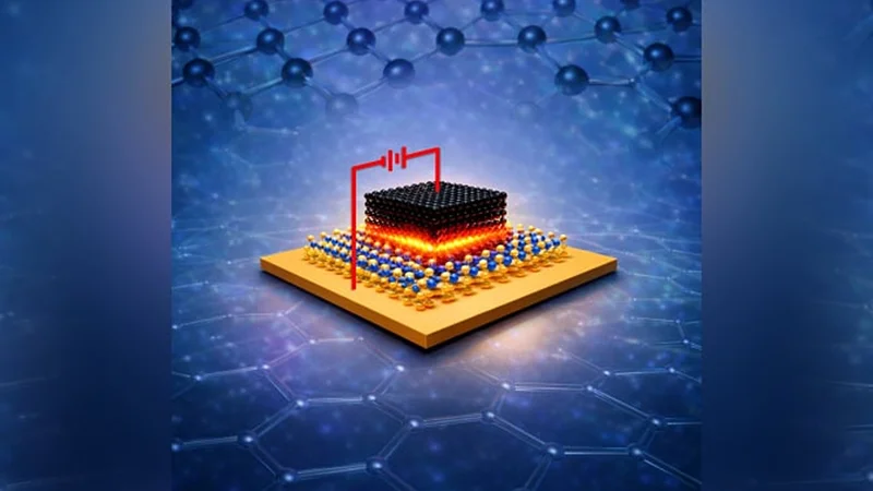
Accurate models of how currents move through anisotropic thin films, made of layered 2D materials, can enable the design of more reliable, high-performance nanoelectric devices. Specifically, the model can help engineers reduce current crowding and spreading resistance, essentially current traffic jams, that occur at vertical electrical contacts that connect with the top of a 2D surface. The study, published in ACS Applied Electronic Materials, was funded primarily by the Air Force Office of Scientific Research.
Anisotropic conductivity causes current traffic jams
Anisotropic conductivity in layered 2D materials means that currents entering from a vertical contact can zoom down the horizontal plane, but they get caught vertically between layers, which are held together by weak van der Waals forces. Charges from a metal contact often get “jammed” near the edges rather than traveling down the speedy horizontal plane, a phenomenon known as current crowding.
Current crowding then causes spreading resistance (also known as constriction resistance) as the current is forced to spread out from a small contact point into a larger material. This is kind of like the traffic jam that would occur if a four-lane highway merged to two lanes before fanning out to six lanes.
Previous spreading resistance models assumed isotropic charge transport, meaning even spreading in all directions. The research team found these models consistently fail for anisotropic 2D materials like molybdenum disulfide (MoS<sub>2</sub>) and graphene, which are commonly used in thin-film devices.
“Contact resistance, especially the contribution from the spreading resistance, is treated as a fitting parameter rather than based on geometry and material anisotropy in the transmission line method or classical diffusion models. For 2D materials, that simplification can hide important physics,” said Md Arifuzzaman Faisal, a doctoral student of nuclear engineering and radiological sciences at U-M and lead author of the study.
An exact field solution to avoid guesswork
To avoid relying on approximations, the research team developed a new exact field solution by using second-order differential equations called Laplace equations. The new model also accounts for the physical dimensions—unlike previous models, which relied on a mathematical simplification assuming materials were sufficiently thick or long.
“We were motivated by the disconnect between traditional contact models and the way current actually distributes in highly anisotropic materials. Bridging that gap is essential if these materials are going to be reliably integrated into real and practical technologies,” said Peng Zhang, an associate professor of nuclear engineering and radiological sciences at U-M and corresponding author of the study.
The researchers used a simulation called the finite-element method to validate accuracy and found excellent agreement with the new model. Next, they proved the model also works in the real world by applying it to experimental data on MoS<sub>2 </sub>thin films and on a wider, thicker substrate called high-oriented pyrolytic graphite. In both cases, the model matched spreading resistance data without using fitting parameters.
As a final step, the researchers backtracked to pinpoint where previous models failed. They found that the previous models work to a certain extent, but fail for ultrathin films or short channels—both critical features of nanoelectronics.
“This work provides a clear and unambiguous method to understand how current actually flows in layered materials, rather than relying on simplified assumptions that only work in limited cases. By explicitly accounting for anisotropic conductivity and realistic device geometry, the model helps the community avoid misinterpreting contact-resistance measurements and offers practical guidance for designing better contacts in 2D electronic devices,” said Zhang.
Increase out-of-plane conductivity in the 2D layer
Using the model, the researchers derived solutions for both planar and disc-shaped thin-film materials to see if geometry influenced anisotropic charge transport. Planar and disc contacts had nearly the same spreading resistance when contact areas were matched, showing the physics is mainly set by the anisotropic charge transport and device dimensions, not the lateral shape of the layer.
Low out-of-plane conductivity, meaning low conductivity vertically between 2D layers, forces most of the current to flow along the contact edges. This significantly increases local current density and leads to local hot spots that threaten device reliability. Increasing out-of-plane conductivity of the 2D layer is the most effective way to reduce spreading and contact resistance.
By strategically adjusting the contact area and thickness of the thin film, engineers can reduce the severity of traffic jams at electrical contacts.
“This model is not just theoretically rigorous but also immediately useful. Researchers can apply it directly to real devices to better understand current crowding, extract meaningful transport parameters, and improve contact design,” said Zhang.
This research was supported by the Air Force Office of Scientific Research (FA9550-22-1-0523; FA9550-20-1-0409).