Lighter Conductors, Higher Conductivity, Industrial Volume: What Dry Phase Patterning Means for Flex Designers
A lighter conductor can change circuit electrical design, its assembly, and its production cost. DP Patterning mechanical approach to flex manufacturing brings those decisions together, with a planned drone demonstration at electronica 2026 offering engineers a closer look.

10 Nov, 2026. 6 minutes read
Saving weight in a drone’s electronics is useful until the change makes the circuit harder to build. A lighter metal still has to carry current. It needs a dependable connection that survives the operating environment, and the finished assembly has to make economic sense when production grows. The attractive material choice can become a negotiation between the layout, the joint and the manufacturing line.
The patterning process sets many of those terms before the first prototype is made. Wet etching commits the circuit to a chemical production sequence. Printing introduces an ink whose electrical performance depends on formulation and processing. Engineers work within those conditions, adjusting the design until its performance and manufacturing requirements agree. Changing how the conductor is formed can reopen choices that otherwise appear settled.
That is the opportunity behind DP Patterning’s Dry Phase Patterning. The Swedish company mechanically cuts a circuit pattern into a metal-coated flexible laminate. At electronica 2026, it will present the process for applications including lightweight defense drone electronics. Its first departure from silver printing happens before the machine even moves.
The Conductor is Already There
Dry Phase Patterning begins with a conductive layer that already has the electrical properties of a metal foil. Aluminium and copper-clad aluminium are central to DP Patterning’s production offering. A flexible carrier such as PET supports the layer. The task is to remove unwanted metal precisely enough to leave a working circuit on an intact substrate.
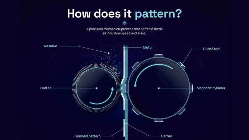
A patterned tool and a milling wheel make that selective removal possible. The cliché, mounted on a rotating cylinder, presses the laminate against the wheel in the areas to be removed. As the web advances, unwanted metal leaves as dry swarf and the conductive pattern remains on the carrier. DP Patterning’s mechanical patterning process runs continuously from roll to roll, with subsequent finishing and assembly completing the part.
The cut removes chemical underetch from the geometry problem, but precision still has to be engineered into the tool and laminate. Line width and clearance must suit the application and remain reproducible as the web moves through the machine. Conductor thickness matters here, too. A foil selected to solve an electrical problem becomes material the cutting process must handle consistently.
A Lighter Metal Brings Another Decision
Aluminium’s low density is attractive in a drone, but matching a copper trace’s resistance takes more cross-section. At the same width and length, the aluminium conductor needs to be thicker because its resistivity is higher. The mass calculation is therefore tied to an electrical calculation from the start. A thinner or lighter-looking laminate on its own cannot establish which assembly makes better use of the weight budget.
The design has room to move because resistance depends on geometry as well as material. For a uniform conductor, increasing width or thickness lowers resistance; increasing length raises it. An interconnect squeezed between components may have little width to spare, which makes thickness more important. An antenna introduces its own geometric constraints. The engineer has to find a conductor that fits the function and then carry that choice into the physical stack.
The comparison with printed silver opens a different opportunity. DP Patterning reports up to 2–3X the conductivity of printed silver inks. Dry Phase Patterning leaves a solid-metal path whose conductivity does not have to be established by drying or sintering an ink. The potential saving starts in the conductor.
In an RFID or NFC design, the foil is useful only as part of an antenna that performs in its final position. Its shape and carrier interact with the rest of the assembly, so lower conductor loss cannot settle the design on its own. A sample should use the proposed substrate and represent how the part will be mounted. The engineer can then test whether changing the conductor preserves the intended RF behaviour and whether that change makes the antenna more economical to produce.
A promising conductor can still meet its most awkward constraint at the terminal. If connecting the foil introduces a difficult assembly operation, part of the weight or cost advantage can disappear there. Copper-clad aluminium addresses that interface by providing a copper surface for soldering while retaining aluminium within the conductor. The designer can investigate a lightweight core with a practical attachment route, then select the substrate and joint protection around the assembly conditions.
The complete stack also has to tolerate the way the circuit bends. An antenna formed once around a housing faces a different duty from an interconnect flexing repeatedly in service. Adding metal to reduce resistance changes the laminate that must accommodate that movement. Material selection, thickness and component attachment need to reach a workable agreement before a successful electrical sample can become a dependable part.
The Saving has to Reach the Finished Part
The process becomes commercially interesting when it removes costs that would otherwise follow every circuit through production. Mechanical cutting eliminates the etching bath and uses minimal water for the patterning operation. The removed metal can be collected for recycling. Because the starting layer is already conductive, ink drying and sintering are also absent from conductor formation.
Those missing operations account for much of DP Patterning’s environmental appeal. DP Patterning reports reductions of up to 98% in energy consumption and CO₂ emissions at the patterning stage compared with conventional etching. That reduction follows a change in the manufacturing route, which avoids the bath, rinsing and associated handling of wet patterning. It brings electronica’s energy-efficiency discussion into the factory, before the circuit ever draws power in a product.
A shorter patterning sequence, however, has to remain economical through finishing and assembly. Yield, protective layers and termination work contribute to the delivered price, while tooling has to be paid for across the production run. Roll-to-roll manufacture provides a route to repeating the pattern at volume, supported by an annual production capacity of 10 million square metres. Early attention to the joint and stack helps keep the simpler process from handing its saving to a harder downstream operation.
DP Patterning’s heater demonstrator with Avery Dennison and IUMAT illustrates that relationship in a finished application. Dry Phase Patterning forms the metal heater circuit, while bonding and integration turn it into an automotive assembly. Here the conductor must deliver a designed resistance to generate heat across the intended area. Battery cell contact systems and flexible interconnects place a different demand on the same manufacturing approach: carrying current while controlling temperature rise. The useful conductor is the one sized for that job.
The Prototype has to Survive Success
Success at the prototype stage can make a process change harder to justify. The circuit has passed its tests, but moving it to another production route may change the dimensions, material stack or assembly that produced those results. Those decisions then need to be revisited just as the programme is trying to grow. DP Patterning supports pilot work and volume production on a common patterning platform, allowing engineers to develop the sample with its eventual manufacturing route already in view.
A revised layout still needs tooling that can reproduce it. A new cliché changes the circuit pattern, and tool preparation and qualification have to fit the development schedule. But the revision returns to the same roll-to-roll architecture, where each run can build on what the previous sample established. Fast pattern changes are useful because they keep design iteration connected to the process expected to manufacture the final part.
Keeping the process consistent solves one scale-up problem, but it leaves the programme dependent on the factory that runs it. A dry mechanical line avoids the etching baths and rinse-water systems required by wet patterning, reducing that part of the infrastructure needed to establish production. DP Patterning’s new Norrköping facility connects that process to European capacity and potential regional manufacturing near customers. The cut enables a simpler production setup; investment and qualification make it a usable source of supply.
The foil choice can reduce another dependency at the same time. When aluminium or copper-clad aluminium meets the circuit’s requirements, silver ink leaves the bill of materials, along with exposure to that input’s price and availability. Base-metal laminates still need to be sourced, but engineering and procurement can assess them against an established European production route. The original material decision now has consequences for what must be purchased, where it can be patterned and how the programme can grow.
A Closer Look at electronica
The drone application brings the value of that connection into focus. Saving conductor mass matters only when the circuit can carry its electrical duty through a reliable joint and into an affordable production run. Dry Phase Patterning gives engineers a way to work across those constraints by changing the operation that defines the conductor. The demonstration is an opportunity to examine how that manufacturing choice translates into a physical assembly.
DP Patterning is in Munich at electronicia 2026, Hall A1, Booth 403, 10–13 November 2026, with a live drone demonstration. Engineers can request samples and book a technical meeting to discuss their own layouts, material stacks and production needs. Seeing the patterned metal, its carrier and its connections together is a useful place to begin exploring what a different manufacturing route could change.