Laser annealing builds an optical isolator into a silicon photonics chip
A laboratory device reaches 13.6 dB of isolation at 1540 nm, with heat confined to a window 700 micrometres across instead of the whole wafer going through a furnace.

23 Sep, 2026. 4 minutes read
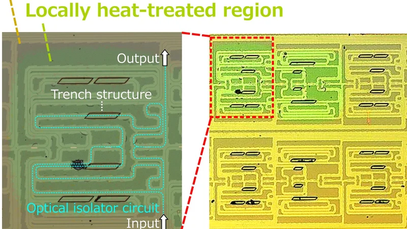
Microscopic image of the optical isolator fabricated and integrated onto a silicon photonics circuit by laser annealing
A way to build optical isolators directly onto silicon photonics chips:
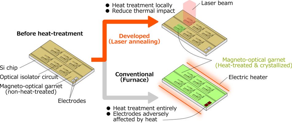
Kyocera and the Research Institute of Electrical Communication at Tohoku University have announced a way to build optical isolators directly onto silicon photonics chips. A 915 nm diode laser crystallises magneto-optical garnet inside a 700 micrometre square region, in place of the whole-chip heat treatment above 600 °C that would damage silicon waveguides and metal electrodes. The demonstrated asymmetric Mach-Zehnder device reaches an isolation ratio of 13.6 dB, which the two organisations describe as cutting back-reflected light by about 95%. The work appeared in IEEE Access on 2 September 2026.[1][2]
Why does it matter
Isolation here comes from interference. A garnet film above the waveguide gives light a different propagation constant depending on which way it travels, so an asymmetric Mach-Zehnder interferometer can be set to combine forward light constructively and backward light destructively. Getting garnet onto silicon has been the obstacle for years. A 2022 review lists high annealing temperature as one of the two material problems in the field, and notes that these have kept optical isolation in discrete modules assembled by physically picking and placing bulk garnet pieces.[3]
The local anneal works: a 915 nm beam held the substrate at 730 °C for 1900 seconds over a 700 micrometre square, and aluminium test pads at the chip edge came through without melting or delaminating. However, the garnet had to be divided into micrometre-scale trenches, because laser annealing an area larger than a square millimetre cracks the film. Those trenches then account for 6.3 dB of the 9.5 dB propagation loss, almost all of it at the trench facets. The step that makes the method possible is the step that costs the light, and the proposed ways out are backfilling the trench with silicon dioxide or removing it altogether.[2]
Set against that, the Faraday rotation of 0.092 degrees per micrometre is a real gain over the same group's earlier laser-annealed Ce:YIG at 0.01, and sits inside the 0.021 to 0.113 that other deposition methods report.[2] Their June 2026 device, built on nanocomposite garnet without laser annealing, reached 18.7 dB of isolation.[4] This one is also not magnet-free: it needs 220 mT in-plane from samarium cobalt magnets, which is the second design problem the 2022 review names. Bonding garnet onto a silicon waveguide reached 21 dB back in 2008, and packaged discrete isolators sell at better than 30 dB for under 1 dB of loss.[2][3][5][6]
Technical specifications: asymmetric Mach-Zehnder isolator, 100 micrometre trench
| Spec | Value |
|---|---|
| Isolation ratio | 13.6 dB at 1540 nm, TM polarisation |
| Insertion loss | 20.4 dB |
| Propagation loss | 9.5 dB |
| Propagation loss breakdown | Trench process 6.3 dB (66%), Ce:YIG loading 2.6 dB (27%), Mach-Zehnder formation 0.64 dB (7%) |
| Faraday rotation | 0.092 degrees per micrometre |
| External magnetic bias | Required. 220 mT in-plane at the chip, from samarium cobalt magnets |
| Magneto-optical film | Ce:YIG, 195 nm thick, ion beam sputtered, no seed layer |
| Waveguide | 180 nm by 550 nm, silicon on insulator, commercial photonics process |
| Trench | 100 by 20 micrometres, short axis tilted 45 degrees |
| Anneal | 915 nm diode laser, 700 micrometre square, 730 °C held 1900 s, below 80 Pa, no scanning |
| Interface | About 10 nm Ce/Fe/Y/SiO2 boundary region at the Ce:YIG and silicon interface |
| Measurement | 1520 to 1610 nm sweep, chip held at 25 °C |
| Product, price, commercialisation date | not stated |
Sources: [1][2]
The loss is the constraint here and it's clear where it appears: two thirds of the propagation loss sits in the trench process, almost all of that at the trench facets. The Ce:YIG contribution traces to the roughly 10 nm interface layer, whose absorption runs three orders of magnitude higher than the crystallised garnet, so both major terms are fabrication artefacts rather than properties of the material. Two constraints sit outside the loss budget and are harder to engineer away: the bias magnets have to fit wherever the chip goes, and the anneal occupied one 700 micrometre square for 1900 seconds without scanning.
Recommended Reading: Silicon Photonics: A Comprehensive Guide to the Future of Optical Communications. Background on the platform, including how silicon waveguides are built and why loss matters.
References
- World's First: Kyocera and Tohoku University Develop Technology to Integrate Optical Isolators Directly onto Silicon Photonics Chips, Kyocera and Tohoku University via Business Wire, 10 September 2026.
- Monolithic Magneto-Optical Mach-Zehnder Isolator Using Laser-Annealed Iron Garnet on a Silicon Waveguide, Sugita et al., arXiv preprint of the IEEE Access paper, 23 July 2026. Published in IEEE Access, 2 September 2026.
- Review of integrated magneto-optical isolators with rare-earth iron garnets for polarization diverse and magnet-free isolation in silicon photonics, Srinivasan and Stadler, Optical Materials Express, 25 January 2022. Peer-reviewed review of why garnet integration is hard.
- Silicon-Compatible Nanocomposite Garnet Enables Better, Simpler Optical Isolators, Tohoku University, 16 June 2026. University summary of the same group's earlier paper in ACS Applied Optical Materials.
- Magneto-optical isolator with silicon waveguides fabricated by direct bonding, Shoji, Mizumoto et al., Applied Physics Letters, 2008.
- Optical Isolator, ScienceDirect Topics. Overview of commercially available packaged isolator performance.
- Monolithic integration of broadband optical isolators for polarization-diverse silicon photonics, Optica, April 2019. Monolithically integrated TE and TM isolators on silicon and silicon nitride.