Integrated Photonics: Comprehensive Guide to Optical Communication
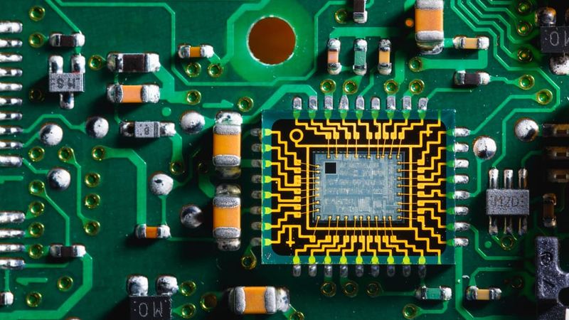
Integrated photonics, also known as planar lightwave circuits or integrated optical circuits, revolutionizes optical communication by leveraging the properties of light to process and transmit information. This cutting-edge technology offers superior efficiency and compactness compared to traditional electronic components, paving the way for faster and more energy-efficient communication systems. With its interdisciplinary nature encompassing materials science, quantum physics, and electrical engineering, integrated photonics presents an exciting and promising field of study and research in today's digital era.

07 Jul, 2023. 17 minutes read
Introduction
Integrated photonics is an innovative technology within the field of optical communication. The technology leverages the principles of light, more specifically photons, to process and transmit information. The power of integrated photonics lies in its ability to perform functions typically carried out by electronic components but with greater efficiency and compactness. Furthermore, its potential for scalability and integration into existing electronic systems paves the way for faster, energy-efficient communication, making it an instrumental technology in today's digital era. As a multidisciplinary field, integrated photonics amalgamates aspects of materials science, quantum physics, and electrical engineering, making it a compelling area of study and research.
2. Core Concepts in Integrated Photonics
The mastery of core concepts in integrated photonics is instrumental in unlocking the full potential of this technology and shaping the future of optical communication. So, let’s take a look at the core concepts that make integrated photonics.
2.1 Waveguides
Waveguides, a fundamental concept within integrated photonics, represent the physical infrastructure that guides light waves from one point to another. Operating as the photonic equivalent of electrical wires, these structures channel light along predefined paths, making them pivotal to integrated photonic devices.
Waveguides are comprised of a core and a cladding. The core, typically made from a material with a high refractive index, is where the light travels. The cladding, with a lower refractive index, surrounds the core and ensures light remains confined within it. The principle of total internal reflection governs the operation of waveguides, ensuring the light propagates along the guide without substantial loss.
The design and geometry of waveguides vary based on the requirements of specific applications. For instance, rectangular waveguides, which comprise straight lines and right angles, are utilized extensively in silicon photonics due to their compatibility with existing semiconductor fabrication techniques.
The size of a waveguide has a direct impact on the wave propagation, defined by the waveguide's mode. A single-mode waveguide, with dimensions roughly matching the light's wavelength, allows one light path or mode. In contrast, a multi-mode waveguide, larger in size, supports multiple light paths. While single-mode waveguides offer higher bandwidth and allow for longer distances due to less modal dispersion, multi-mode waveguides are often more tolerant to alignment errors, which can be advantageous in certain applications.
Waveguides, beyond their basic role of directing light, also exhibit a variety of more complex behaviours. For instance, in the field of nonlinear optics, the intensity of light within a waveguide can influence the waveguide's refractive index, leading to a multitude of nonlinear phenomena. These properties are fundamental to devices like optical amplifiers and photonic logic gates.
2.2 Modulators
In integrated photonics, modulators serve a critical role in manipulating light properties to carry information. They function by altering light waves in a manner analogous to how electronic devices modify electric signals, essentially encoding data onto light waves. This manipulation primarily occurs through changing properties like amplitude, phase, or frequency of the light wave.
Electro-optic modulators, a commonly used variety in integrated photonics, leverage the electro-optic effect, where an applied electric field results in a change of the refractive index of a material. The most widely used class of these devices are Mach-Zehnder modulators, which function based on the interference of two light paths or arms. By applying an electric field, the refractive index of one arm can be changed, creating a phase shift between the two arms. This results in the interference at the output either reinforcing or cancelling the light, enabling amplitude modulation.
High-speed data transmission often uses phase modulation as it is less susceptible to noise and loss compared to amplitude modulation. Quadrature Phase Shift Keying (QPSK) is a modulation scheme which uses four different phase shifts to represent digital data, enabling the transport of more information per symbol, and is widely used in high-speed optical communication.
Frequency modulation, another important method of optical modulation, is less common in integrated photonics due to the relatively large spectral width required. However, this method sees application in certain areas, such as the generation of frequency combs, which are essential tools in high-precision spectroscopy and optical clocks.
Modulators based on absorption changes, such as electroabsorption modulators, also exist. These devices operate by modifying the absorption spectrum of a material using an electric field, allowing the modulation of light intensity.
The performance of an optical modulator is characterized by factors such as its modulation depth (the extent of light property change), speed (the rate at which the light property can be changed), and power consumption. Modern integrated photonic platforms are capable of modulator speeds beyond 50 GHz, with modulation voltages of a few volts, making them an essential component in high-speed, energy-efficient optical communication systems.
2.3 Photodetectors
Photodetectors play a crucial role in integrated photonics by translating optical signals back into electrical signals, hence enabling the interaction between electronic and photonic systems.
One of the most prevalent types of photodetectors is the photodiode. Photodiodes operate using a p-n junction, a boundary within the device between p-type and n-type semiconductor materials. When a photon with sufficient energy strikes the junction, it can promote an electron from the valence band to the conduction band, leaving behind a hole in the valence band. This electron-hole pair then contributes to a photocurrent under an applied reverse bias voltage.
In integrated photonics, one widely used category of photodiodes is the avalanche photodiode (APD). APDs operate under a high reverse bias voltage, allowing for a phenomenon called impact ionization. When an electron gains enough energy from the high electric field, it can knock other electrons into the conduction band, resulting in an "avalanche" of electron-hole pairs and thus a high gain, or multiplication, of the photocurrent. This effect enables the detection of very weak optical signals.
Another significant category of photodetectors is the pin photodiode. Pin photodiodes have an intrinsic (i) layer sandwiched between p-type and n-type layers, which increases the volume of the device where electron-hole pairs can be created. This results in a higher quantum efficiency, the ratio of electrons in the photocurrent to incoming photons, compared to a simple p-n junction photodiode.
The responsivity of a photodiode, defined as the ratio of photocurrent to optical power, is a key parameter for assessing the performance of a photodetector. It determines how efficiently a photodetector can convert optical power into an electrical signal. Other important parameters include speed, noise, and wavelength sensitivity.
Optical receivers in integrated photonics commonly include a photodetector along with a transimpedance amplifier, which converts the current signal from the photodetector into a voltage signal and amplifies it. This integrated system allows for high-speed, high-sensitivity detection of optical signals, critical in applications such as optical communication systems.
2.4 Planar Lightwave Circuits:
Planar Lightwave circuits are flat, chip-based circuits that manipulate and control the propagation of light signals. PLCs are fabricated using thin film deposition and lithography techniques, allowing for the precise integration of various optical components on a single chip or substrate.
PLCs consist of waveguides, which are thin optical channels that guide and confine light signals, as well as other passive and active components such as splitters, couplers, filters, modulators, and detectors. These components are designed and arranged on the chip to perform specific functions, such as routing, splitting, combining, filtering, and modulating light.
The waveguides in PLCs are typically made of high-refractive-index materials, such as silicon or silica-based materials, which enable efficient light confinement and low propagation losses. The compact and planar nature of PLCs allows for high-density integration of optical components, resulting in smaller form factors, improved performance, and cost-effective manufacturing.
3. Key Technologies in Integrated Photonics
The advancement of integrated photonics has been made possible by the development of various technologies. These technologies leverage different materials and techniques to fabricate photonic devices and circuits, each with its unique advantages and limitations.
3.1 Silicon Photonics
One of the most prominent technologies is silicon photonics. This technology utilizes the silicon-on-insulator (SOI) substrate, which consists of a thin silicon layer on top of an insulating layer of silicon dioxide, all on a silicon substrate. The top silicon layer is where photonic devices are fabricated, and the silicon dioxide layer acts as a lower cladding layer for waveguides, confining light within the silicon.
Silicon has several advantages for integrated photonics. First, it has a high refractive index, which enables strong light confinement and thus small device sizes. This is crucial for high-density integration of photonic devices on a chip. Second, silicon is transparent at telecommunications wavelengths (around 1.3-1.6 µm), allowing for low-loss transmission of optical signals.
The high refractive index contrast between silicon (around 3.5) and silicon dioxide (around 1.45) in the SOI substrate also allows for sharp bends in waveguides with low loss, further enabling compact device designs. This is particularly important in applications where space is a premium, such as data centers and telecommunications systems.
Moreover, silicon is compatible with complementary metal-oxide-semiconductor (CMOS) technology, which is the standard technology for fabricating electronic circuits. This compatibility allows for the use of mature and cost-effective CMOS fabrication processes to make silicon photonic devices. In addition, it allows for the co-integration of electronic and photonic devices on the same chip, paving the way for hybrid electronic-photonic systems.
Despite its advantages, silicon photonics also faces several challenges. Silicon has a weak second-order optical nonlinearity due to its centrosymmetric crystal structure, which limits its functionality for certain applications, such as frequency conversion and optical switching. Silicon is also not an efficient light emitter or detector due to its indirect bandgap. This necessitates the integration of other materials, such as germanium or III-V semiconductors, for light emission and detection.
Furthermore, silicon photonic devices can suffer from temperature-dependent performance due to the thermo-optic effect in silicon. This effect can cause shifts in the resonant wavelength of resonant devices and variations in the effective refractive index of waveguides with temperature, potentially affecting the stability of optical signals. Various techniques, such as thermal tuning and athermal device designs, have been developed to mitigate this issue.
3.2 Indium Phosphide Photonics
Another major technology in the integrated photonics landscape is Indium Phosphide (InP) photonics. This material system is based on InP and its associated ternary (InGaAs, InAlAs) and quaternary (InGaAsP, InAlGaAs) compounds.
Indium phosphide offers a unique advantage in photonics due to its direct bandgap, which allows for efficient light emission. This is in contrast to silicon, an indirect bandgap material, which is inefficient at emitting light. Consequently, InP can be used to create efficient light sources, such as lasers and light-emitting diodes (LEDs), directly integrated on the photonic chip. The wavelength of the emitted light can be precisely engineered by adjusting the composition of the ternary and quaternary compounds, covering a broad range from 1.2 to 1.6 µm, which includes the telecommunications bands.
In addition to light sources, InP can also be used to fabricate various other photonic devices, such as modulators and photodetectors. The electro-optic effect in InP and its compounds, which involves the change in refractive index with applied electric field, enables high-speed modulation of light. The direct bandgap and the high absorption coefficient of InP and its compounds allow for the creation of efficient photodetectors.
Furthermore, InP-based materials also exhibit strong second and third-order optical nonlinearities, which can be exploited for wavelength conversion, signal regeneration, and the generation of entangled photon pairs for quantum information applications.
Despite these benefits, InP photonics faces certain challenges. The fabrication process for InP devices is more complex and expensive than that for silicon devices, primarily due to the need for epitaxial growth of high-quality InP-based materials. Additionally, the integration of InP devices with electronic circuits on silicon is not straightforward and typically requires complex hybrid integration techniques.
Moreover, similar to silicon, InP devices also suffer from temperature-dependent performance, which needs to be managed for stable operation. InP is also mechanically brittle, which could present challenges in the packaging and deployment of InP photonic devices.
3.3 Hybrid Integration
Hybrid integration in integrated photonics represents an advanced approach to combine the strengths of different material systems and device technologies. Instead of trying to achieve all photonic functions within a single material system, which could be difficult due to material limitations, hybrid integration involves bringing together different photonic components made from different materials onto a common platform.
For example, silicon, which is a dominant material in the electronics industry due to its excellent electronic properties, has limited ability to generate light because of its indirect bandgap. On the other hand, materials like Indium Phosphide (InP) and Gallium Arsenide (GaAs) have direct bandgaps and are efficient light emitters, but their electronic properties are not as superior as silicon. In a hybrid integration approach, light-emitting devices made from InP or GaAs can be integrated with silicon photonic circuits to achieve a system that can efficiently manipulate both electronics and photons.
There are several methods for hybrid integration. One common method is bonding, where photonic devices fabricated in different material systems are brought into close contact and adhered together using an adhesive layer. For instance, wafer bonding can be used to adhere an InP-based laser to a silicon waveguide. Here, a very thin bonding layer is typically used to ensure good optical coupling between the devices.
Flip-chip bonding is another hybrid integration method, where a photonic chip is flipped and bonded onto a host substrate such that the active layers of the photonic chip are in close proximity to the host substrate. This allows for efficient optical, electrical, and thermal interaction between the devices on the photonic chip and the host substrate.
Another important aspect of hybrid integration is the alignment and coupling of devices. Sub-micron accuracy is typically required to ensure efficient coupling of light between devices. This can be achieved using passive alignment features integrated into the device design, or active alignment using precision equipment.
However, hybrid integration is not without challenges. It often requires complex fabrication processes and can increase the cost and footprint of the integrated photonic system. Moreover, the thermal, electrical, and mechanical compatibility of different materials and devices needs to be carefully managed.
4. Role of Integrated Photonics in Different Industries
The role of integrated photonics extends beyond optical communication and encompasses diverse industries. Its impact can be seen in telecommunications, data centers and medicine. By enabling faster, more efficient data transmission, processing, and sensing, integrated photonics is transforming industries and paving the way for technological advancements. In this section, we will explore the significance of integrated photonics in different sectors and how it is shaping the future of various industries.
4.1 Telecommunications
The telecommunications industry is able to transmit, manipulate, and detect light signals has underpinned many advances in high-speed data communication and network infrastructure.
In fiber-optic communication systems, integrated photonics offers an efficient means of converting electrical signals into optical signals and vice versa. Modulators play a critical role in this conversion process. A stream of digital data, represented by voltage levels, modulates a continuous light beam from a laser source, encoding the data into optical form for transmission over fiber optic cables. Photodetectors on the receiving end translate the optical signals back into their electrical form. Due to the vast capacity and low signal degradation of light transmission, these systems have become the backbone of global telecommunications infrastructure.
The growing demand for higher data rates and lower power consumption has led to the development of advanced modulation schemes, such as Quadrature Phase-Shift Keying (QPSK) and Quadrature Amplitude Modulation (QAM). These methods encode information not only in the intensity of the light but also in its phase and polarization, significantly increasing the amount of data that can be transmitted per second. For instance, coherent communication systems, utilizing QPSK modulation, can achieve data rates up to 100 gigabits per second per wavelength channel.
Optical Add-Drop Multiplexers (OADMs), devices capable of adding, dropping, or rerouting different wavelength channels in a dense wavelength division multiplexed (DWDM) system, are another key application of integrated photonics in telecommunications. In a typical DWDM system, a multitude of different wavelength channels, each carrying a separate data stream, are combined and transmitted together over a single optical fiber. OADMs allow for selectively adding or dropping individual wavelength channels at different points along the transmission line, thus enabling flexible network configurations.
Reconfigurable Optical Add-Drop Multiplexers (ROADMs), a more advanced version of OADMs, have been instrumental in creating agile and dynamic optical networks. With the capability to remotely reconfigure the routing of wavelength channels, ROADMs eliminate the need for manual reconfiguration, reducing operational cost and downtime.
4.2 Data Centers
The exponential growth of digital content, cloud services, and internet traffic has led to a surge in the scale and complexity of data centers. These massive infrastructures are responsible for storing, managing, and processing vast amounts of data generated every day. Integrated photonics has emerged as a pivotal technology in the data center landscape, helping to enhance the speed, efficiency, and scalability of data center operations.
Interconnect technology forms the backbone of data centers, linking various computing resources and enabling data exchange. With traditional copper-based interconnects struggling to keep up with increasing bandwidth requirements, photonic interconnects offer an effective solution. Optical interconnects, powered by integrated photonics, provide high-speed data transmission over longer distances with lower power consumption. They overcome the limitations of electrical interconnects such as signal attenuation and electromagnetic interference.
Silicon photonics, in particular, is recognized for its potential in data center applications due to its compatibility with existing CMOS technology and the ability to integrate electronic and optical functions on the same chip. For example, silicon photonic transceivers have shown promising results in meeting the demands of high-speed, low-power, and high-density interconnects in data centers. Current commercial silicon photonic transceivers offer data rates up to 400Gbps and have the potential to reach into the terabit range in the future.
Within a data center, optical interconnects are utilized in different tiers of the network hierarchy. At the top tier, where the distances are longer and data aggregation is higher, coarse wavelength division multiplexing (CWDM) and dense wavelength division multiplexing (DWDM) technologies are commonly used. These technologies transmit multiple data streams concurrently over the same fiber, each stream on a distinct wavelength, maximizing the bandwidth utilization of the optical fiber.
At the rack level, the demand is for shorter reach but higher density interconnects, which has led to the emergence of parallel single-mode fiber (PSM) and multi-mode fiber (MMF) solutions. These solutions employ multiple parallel optical channels for data transmission, each channel operating at a lower data rate, allowing for a cost-effective way to achieve high total bandwidth.
Apart from interconnect technology, integrated photonics also holds promise for on-chip optical communication, potentially revolutionizing the way data is transferred within a chip. By replacing electrical wires on a chip with optical waveguides, data could be transported across different parts of the chip at the speed of light, leading to significant improvements in processing speed and energy efficiency.
As the need for data storage and processing continues to grow, the role of integrated photonics in data centers will become increasingly significant. Through advancements in this technology, data centers can continue to increase their capacity and performance, meeting the demands of an ever more digitally connected world.
4.3 Lidar:
The role of integrated photonics in the automotive sector has so far been modest, but its potential is extensive and touches all aspects of the vehicle and system design. One promising area is in Lidar (Light Detection And Ranging) systems, used to assist autonomous vehicles to ‘see’. Currently, these laser-based systems are extremely expensive, often costing more than tens of thousands of dollars for a single system which limits their commercial availability. Additionally, these early systems carried with them concerns about their reliability, eye safety (due to the close to visible range wavelength regions used), and limited accuracy (given the relatively simple ranging schemes possible). Integrated photonics offers the opportunity to reduce this cost and increase system safety.
The Doppler effect is the term given to the phenomena of the frequency of a wave changing when its source is in motion relative to an observer. Frequency-modulated continuous-wave (FMCW) Lidar works by measuring the doppler shift coherently, preventing interference from sunlight and other lidar systems. This system design offers distance resolution but comes at the cost of low acquisition speed and requires a highly coherent, as well as precisely chirped, laser source. Researchers from the Swiss Federal Institute of Technology have outlined how a novel approach multiplexes a single FMCW laser using a high-quality silicon-nitride microresonator on a photonic chip.
Recommended Reading: Simulation accelerates the development of Photonic Integrated Circuits for automotive applications
4.4 Medicine
Integrated photonics is making significant strides in the field of medicine, where it has potential to revolutionize disease detection, imaging techniques, and surgical procedures. The appeal of this technology lies in its ability to miniaturize and integrate various optical components on a single chip, allowing for high-precision, non-invasive, and real-time medical applications.
Optical biosensors are one example of how integrated photonics can enhance disease detection. These biosensors leverage evanescent wave sensing, where a small fraction of light propagating through an optical waveguide interacts with the surrounding medium. When this medium includes biological samples, specific interactions with the evanescent field can provide information about the presence and concentration of target biomolecules, leading to early disease diagnosis. Silicon photonics-based biosensors, thanks to their high sensitivity and compatibility with CMOS technology, have successfully detected proteins, nucleic acids, and even cancer cells at extremely low concentrations, as low as a few parts per billion.
Integrated photonic technology also enables Optical Coherence Tomography (OCT), a non-invasive imaging technique. It uses light to capture micrometer-resolution images from within optical scattering media, like biological tissues. In ophthalmology, OCT devices provide high-resolution three-dimensional images of the retina, contributing significantly to the early diagnosis and management of eye diseases such as macular degeneration and glaucoma. Photonic integrated circuit (PIC) based OCT systems have seen considerable success due to their compact size, lower cost, and improved reliability.
Another area of medicine where integrated photonics shows great promise is in endoscopic procedures. A prominent application of this is the photonic integrated chip (PIC)-based optical biopsy. Traditionally, a biopsy involves removing tissue for examination, which can be invasive and risky. A PIC-based optical biopsy uses a miniature OCT system, integrated onto a small endoscope that can be inserted into the body. This allows for non-invasive, real-time imaging and analysis of tissue at a cellular level, aiding in immediate diagnosis and reducing the need for traditional biopsy procedures.
The application of integrated photonics extends to laser surgery as well. High power lasers are used in various medical procedures, ranging from dermatology to neurosurgery. The integration of these lasers onto photonic chips could lead to more compact, efficient, and precise laser systems. For instance, the integration of a high-power, ultrafast laser on a chip could pave the way for 'bladeless' surgery, where tissue is precisely removed layer by layer, without any physical contact.
5. Conclusion
Integrated photonics, with its promising characteristics such as smaller size, lower power consumption, and higher bandwidth, is set to redefine several industry domains. From telecommunications and data centers, to medical technologies, the technology's penetration is expanding rapidly. The advent of silicon photonics and indium phosphide photonics have further propelled the growth of integrated photonics by offering enhanced integration capabilities and high performance. Hybrid integration, a combination of different photonic platforms, is poised to address some of the challenges associated with individual materials, making this technology even more versatile.
The road ahead for integrated photonics is filled with abundant opportunities, especially as research and development in the field continue to advance. As a society, we stand on the brink of a new technological revolution with integrated photonics at its core, promising to transform our industries, our infrastructure, and our everyday lives. The journey of integrated photonics has just begun, and its potential is limited only by our imagination.
6. Frequently Asked Questions (FAQs)
What is integrated photonics?
Integrated photonics refers to the technology where multiple photonic components are integrated onto a single chip, similar to how multiple transistors are integrated onto a single silicon chip in electronics. These photonic components can include lasers, modulators, waveguides, detectors, and more.
What is the significance of silicon in integrated photonics?
Silicon is the fundamental material used in electronics, and using it in photonics offers the ability to leverage existing silicon manufacturing infrastructure. This results in cost-efficient mass production. Moreover, silicon is transparent to infrared light, which is the region of the spectrum where most telecommunication applications operate.
What is the role of integrated photonics in telecommunications and data centers?
In telecommunications and data centers, the demand for higher data rates and lower power consumption is continuously increasing. Integrated photonics can address these demands by providing higher bandwidth, lower power consumption, and smaller physical footprint. It also provides the capacity to manage vast amounts of data with decreased latency.
How is integrated photonics applied in the field of medicine?
Integrated photonics has found application in various medical fields, including disease detection, imaging, and surgical procedures. For example, it enables the development of biosensors for early disease detection, optical coherence tomography for high-resolution imaging, and endoscopic procedures for non-invasive biopsy and surgeries.
What is hybrid integration in the context of integrated photonics?
Hybrid integration refers to the combination of different photonic platforms within a single photonic integrated circuit. This approach is used to overcome the limitations associated with individual materials, allowing for more versatile integrated photonic devices.
References:
https://www.sciencedirect.com/topics/engineering/optical-telecommunication
https://www.mdpi.com/1996-1944/14/23/7125
https://www.sciencedirect.com/topics/earth-and-planetary-sciences/quaternary-alloy