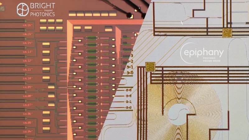
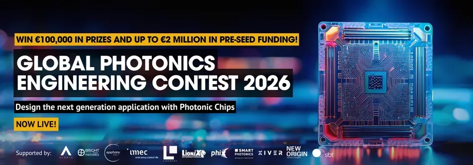
Inside Photonic Chip Design: Perspectives from Epiphany Design and Bright Photonics
A Q&A with Epiphany Design and Bright Photonics on transforming PIC concepts into manufacturable systems, with practical guidance for teams participating in the Global Photonics Engineering Contest 2026.

29 Jun, 2026. 10 minutes read
Introduction
Integrated photonics is steadily moving from research labs into real-world applications, with growing demand across communications, sensing, AI, and beyond. As this transition accelerates, the complexity of designing photonic integrated circuits (PICs) has also increased, spanning multiple material platforms, packaging approaches, and system-level requirements.
Photonic design houses play a critical role in the value chain towards PIC-integrated applications. They bridge the gap between concept and manufacturable product, helping teams understand platform choices, design constraints, and the realities of fabrication and integration.
This article features a short Q&A with experts from two European design houses: Epiphany Design and Bright Photonics. While Epiphany focuses on platform-agnostic design and system-level decision-making, Bright emphasizes structured design flows, verification, and manufacturability.
Through their insights, this piece aims to provide practical guidance for teams participating in the Global Photonics Engineering Contest 2026, highlighting what it takes to move from an idea to a working, scalable integrated photonic system.
Bright Photonics on Scalable PIC Innovation
Bright Photonics enables scalable, predictable, and accessible PIC innovation. The company provides end-to-end integrated photonic development services and acts as the invisible engine behind PIC-enabled products, startups and advanced technology programs.
With more than 15 years of specialized experience, an optimized design platform, and in-house test capabilities, Bright Photonics has delivered well over a thousand PIC designs across silicon photonics, indium phosphide, silicon nitride, glass, and custom hybrid platforms. The company has contributed to hundreds of projects and supported more than fifty startups by helping them understand, structure, and solve their design challenges. The portfolio includes advanced integrated photonic building blocks such as modulators, lasers, switches, polarization controllers, and fiber-coupling elements.
A core part of Bright Photonics' expertise lies in PIC application analysis and feasibility assessment. The company helps customers navigate a complex and rapidly evolving ecosystem by defining optical subsystems. The feasibility work involves evaluating a broad landscape of suppliers, technologies, hybrid architectures, and assembly concepts before the most viable solution emerges.
In integrated photonics, materials, processes, and suppliers are not interchangeable. A technology or provider cannot simply be swapped without affecting the performance and reliability of the full system. High-level comparisons between material systems or providers tend to be too simplistic for real-world decision-making. Bright Photonics takes into account cross-domain constraints like thermal behavior, electrical interfaces, assembly constraints, cost, risk, and long-term scalability. During a feasibility process, the company embraces flexibility and exploration at the start. Toward the end Bright Photonics narrows the options down into a documented and consistent system-requirement specification.
By reducing technical uncertainty and making complexity manageable, Bright Photonics helps ensure that the chosen development path is not only technically sound but also manufacturable, scalable, and ready for real-world impact.
Peter (PhotonDelta): How would you define your primary value proposition in today’s integrated photonics ecosystem?
Ronald (Bright Photonics): Bright Photonics delivers platform thinking from concept to testing. We provide a predictable, structured, and reliable PIC development process, bringing stability to an otherwise chaotic R&D phase, which can be a common trap for startups. Within a fully independent search for suppliers, technologies, and circuit solutions, we guide customers from early-stage concepts to advanced, production-ready designs using a disciplined explore-design-validate flow. The result is a fully documented, cost-effective, and manufacturable solution tailored to the customer's needs, whether they require an initial feasibility study, a validated module, volume testing, or something in between.
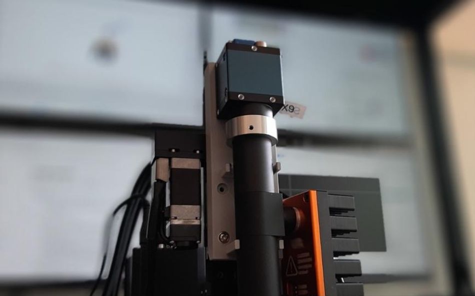
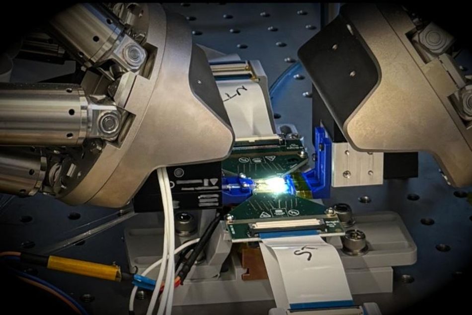
Our in-house digital twin, test and validation capabilities support both real and virtual building-block qualification, PIC-level validation, and early KGD testing; all essential steps for bringing reliable photonic products to market. Customers are welcome to visit our lab to evaluate their systems during die-level testing, gaining direct insight into performance and risk factors as their designs move toward product readiness.
Peter (PhotonDelta): How does your service model help clients move from concept to a verified, manufacturable photonic chip with minimal iteration risk?
Ronald (Bright Photonics): Our PIC development flow begins by systematically capturing all the client’s system-requirement specifications in an iterative process with the client. The design phase combines in-house optimized software with rigorous circuit-level validation. Test and packaging constraints are built into the design cycle from day one, avoiding late-stage surprises. By closing the loop with our test facilities, the entire design flow functions as a standardized development platform.
Relying on these standardized methods rather than individual designer intuition allows us to minimize iteration risk and ensure consistent, scalable outcomes. Furthermore, our simulations proactively account for manufacturing tolerances, calibration procedures, and the specific impact of lab equipment on test results.
Peter (PhotonDelta): Why is the Design for Manufacturing (DfM) approach necessary and essential?
Ronald (Bright Photonics): For PICs to be adopted at the same scale as electronics, the industry must meet equally strict expectations for reliability, traceability, and compliance. Bright Photonics applies auditable, standards-driven processes aligned with the rigorous requirements of sectors such as automotive, aerospace, and medical technology. That means traceability from system specification to PIC architecture to test plan.
In this context, DfM is not optional. It is the bridge between research-grade photonics and industrial-grade products. For a startup, access to this discipline can make the difference between early failure and long-term survival. A critical part of our approach is understanding the true capabilities of foundries and assembly houses worldwide with respect to a customer’s needs. We systematically assess technology, maturity, and process stability. Through quality assurance, we treat acceptable risk as a baseline design constraint, not as an afterthought.
In most products, photonics is not the most expensive component, but it is often the riskiest. PICs typically define the core functionality of the entire system. This means that small variations in process, packaging, or supplier choice can cascade into major system-level failures. Bright Photonics identifies these risks early, quantifies them, and engineers solutions that remain robust under real-world manufacturing conditions. As always in integrated photonics, every detail matters.
Peter (PhotonDelta): Which emerging application areas will drive the next wave of demand for advanced PIC design expertise?
Ronald (Bright Photonics): Design demand growth will ultimately come from cross-market breadth rather than a single killer application. Emerging areas such as quantum communication, medical sensing and satcom all rely on the same maturing integrated-photonic infrastructure, which is currently most strongly boosted by AI-driven datacom. The ecosystem needs a mature, quality-controlled design and development platform that can transfer across different markets to meet demand.
Projects range from one-month sprints to complex multi-year programs. For design demand, project size and complexity often matter more than project count.
Peter (PhotonDelta): How can teams use Process Design Kits (PDKs) and building blocks without limiting innovation?
Ronald (Bright Photonics): Qualified PDKs with compact models, combined with software that supports multiple designers and multiple technologies within one project, do not constrain innovation. They unlock it. With our Nazca Design and Nazca Cloud platforms, we extend the traditional PDK into a digital-twin and virtual-lab environment.
Instead of only providing validated PDK building blocks, the digital-twin captures system-level behavior, layout-dependent effects, and cross-technology integration. The validated PDK models provide predictability, while custom models and architectural exploration add the flexibility needed for innovation. This enables teams to explore architectures freely while staying aligned with system-level requirements from the start.
Peter (PhotonDelta): What advice would you give teams entering the Global Photonics Engineering Contest 2026?
Ronald (Bright Photonics): If you are serious about the end result of your PIC development path, challenge every assumption. In integrated photonics, confidence should come from evidence, not just enthusiasm. Ask for numbers, ask for proof, ask for data, and make sure claims are backed by real performance where possible.
Decide early whether your goal is to learn to drive or to win the race. Both paths are valid, but they require very different choices and very different levels of engineering maturity. Teams that succeed are the ones who stay grounded in verifiable data and choose partners who can demonstrate results, not just promise them.
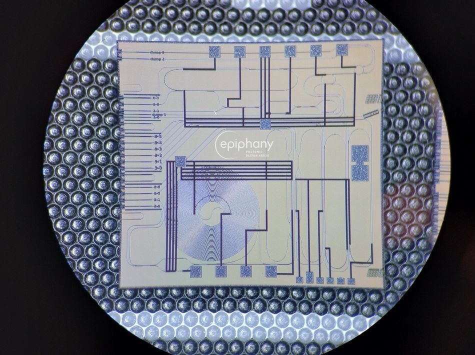
Epiphany Design’s System-Level Approach to Photonic Integration
Epiphany Design is an independent, platform-agnostic photonic IC design house based in the Netherlands, founded by experts with over 35 years of combined experience across the full value chain of integrated photonics. The company offers three core services: PIC design, foundry enablement, and cross-platform hybrid integration, guiding customers from initial concept through to a verified, manufacturable product.
Jörn Epping, founder of Epiphany Design, has extensive experience across photonics and quantum technologies. Before founding Epiphany, Jörn worked at QuiX Quantum as head of R&D hardware and managing director of its German subsidiary as well as project manager at LioniX International. He received his PhD from the University of Twente on integrated nonlinear photonics.
Peter (PhotonDelta): How would you define Epiphany’s primary value proposition in today's integrated photonics ecosystem?
Jörn (Epiphany Design): The integrated photonics ecosystem is growing fast but remains fragmented in many aspects. There are many technology platforms, many foundries, many packaging approaches, and navigating it all takes experience that most teams simply don't have in-house yet. That's where we come in.
Our value is in making the right connections: between application and technology, design and manufacturing, idea and product. We offer platform-agnostic integrated photonic design services, which means we don’t push customers toward a particular foundry or material system. We listen, understand constraints, and then give honest, unbiased recommendations on what will actually work for the final product.
Peter (PhotonDelta): How does your service model help clients move from concept to a verified, manufacturable photonic chip with minimal iteration risk?
Jörn (Epiphany Design): Our ambition is simple: get it right the first time, and we have a track record to back that up.
Design-for-Manufacturing is built into our workflow from day one. It shapes the decisions we make throughout the early design process: yield, packaging compatibility, testability, and assembly. This is the core of what we call our ABCD approach—Assembly-Based Chip Design, which keeps the full downstream process in view from the very first design choices.
Beyond the design itself, we go further and offer what we call “Supply Chain Services,” meaning we support our customers throughout the entire PIC development project. In some instances, we visit customers on-site to measure the chips together. It’s part of our commitment to the project.
Peter (PhotonDelta): Why is the DfM approach necessary and essential?
Jörn (Epiphany Design): As volumes grow, every design decision that ignores yield, assembly, or testing complexity becomes a cost.
Peter (PhotonDelta): Epiphany works across multiple PIC platforms and material systems. How do you guide customers in selecting the right technology, or combination of technologies, for a specific application?
Jörn (Epiphany Design): The first thing we do is listen. Every project comes with its own requirements and constraints: performance targets, cost boundaries, timelines, and sometimes existing investments in a particular platform.
Then we bring our perspective. Some platforms are a clear fit for certain applications; others involve trade-offs that are worth understanding before committing. Increasingly, the most interesting solutions are not single-platform: combining materials like indium phosphide for active functionality with silicon nitride for low-loss routing, for example, opens up performance possibilities that neither platform offers alone.
The end goal always shapes the choice. For those looking to explore the landscape before engaging with us directly, we’ve also developed a Guide to PIC Materials on our website, with structured, practical information and comparisons across platforms.
Peter (PhotonDelta): You have developed modular building blocks such as the Hybrid Laser Design Module. Can you tell us something about that? How do reusable, pre-validated components benefit your customers?
Jörn (Epiphany Design): The Hybrid Laser Design Module came directly from a need we saw repeated across projects: laser integration is one of the most complex and time-consuming parts of a PIC design, and most teams are starting from scratch every time.
We developed a platform-agnostic laser building block that can be integrated into almost any PIC layout, eliminating the need to design the laser from scratch and significantly reducing iteration risk at one of the most critical points in the design. For many projects, this translates directly into months saved in time-to-market.
What makes it practical is that we offer a demo unit—a fully assembled laser demonstration module that customers can test and measure before integrating it into their own system.
This module is already in use, with customers shipping products built around it. That reflects both the maturity of the solution and our broader commitment to enabling commercial outcomes.
Peter (PhotonDelta): From specification to packaging, where do PIC developers most often underestimate complexity?
Jörn (Epiphany Design): If we had to point to one area, it’s the step from a working chip to a working module.
Many teams don’t think about packaging constraints early enough in the design phase, which creates real problems later. But what’s even more underestimated is the full system integration challenge: combining the photonic chip with control electronics, optical interfaces, thermal management, and everything else needed to make the system function reliably in the real world.
Peter (PhotonDelta): For teams entering the Global Photonics Engineering Contest 2026, what early choices will most strongly influence whether a design can realistically move from concept to fabrication?
Jörn (Epiphany Design): As part of the jury in last year’s contest, we’ve seen a wide range of ideas, and the ones that translated most successfully into real applications are those that kept the end goal in view from the very beginning.
Our advice to every team: the chip is a component in a system, and the system is what creates value. Think about how your PIC becomes a product from day one, and design with that destination in mind.
Key Takeaways for Contest Participants
While Epiphany emphasizes system-level thinking, platform flexibility, and early architectural decisions, Bright Photonics approaches PIC development through structured design flows, validation, and manufacturing discipline including testing. Together, these perspectives highlight two essential dimensions of photonic chip design: choosing the right direction early and executing it reliably through to production.
For teams participating in the Global Photonics Engineering Contest 2026, the insights shared by both design houses point to a few consistent themes:
Think beyond the chip: A PIC is only one part of a larger system. Consider packaging, electronics, and end-use conditions from the beginning.
Choose the right platform early: Material and foundry decisions shape performance, cost, and scalability.
Design for manufacturing from day one: Ignoring yield, testability, and assembly early can lead to costly redesigns later.
Leverage existing building blocks: Pre-validated modules and PDK components can significantly reduce risk and development time.
Balance innovation with realism: Strong ideas succeed when they are grounded in what can be fabricated, tested, and scaled.
Prioritize execution over ambition: A well-implemented design often outperforms a more ambitious concept that cannot be reliably realized.
LEARN MORE AND PARTICIPATE NOW
Conclusion
As integrated photonics continues to mature, the role of design expertise becomes increasingly central to translating ideas into working systems. The perspectives from Epiphany Design and Bright Photonics reflect two distinct but equally important aspects of this process: making the right architectural choices early and ensuring those choices can be executed reliably at scale.
For teams entering the Global Photonics Engineering Contest 2026, success will depend not only on innovation but also on the ability to design with the full development pathway in mind, from concept to manufacturable, real-world solution.