How Physical Unclonable Functions (PUFs) are Creating Trust
This article discusses a technology called physical unclonable functions (PUFs) and shows how this technology can help chip vendors and device manufacturers to generate and securely store cryptographic keys that will keep their devices, data, IP, and systems safe from attackers.
Last updated on 08 Sep, 2020. 11 minutes read
At the core of any device’s security architecture is a cryptographic root key. From this root key additional keys can be derived for authenticating the device, validating software, and encrypting sensitive data. Every device that contains something of value (e.g. data or IP) or that is connected to a network needs these keys to operate securely. Since these keys are the anchor of trust for a device, they should never fall into the hands of adversaries who could be looking to steal sensitive data, copy valuable IP, or disrupt connected systems. However, generating these cryptographic keys and storing them securely on a device is far from trivial. PUFs are a technology that provides a secure mechanism for generating and storing cryptographic keys.
What is a Physical Unclonable Function?
A very good definition of physical (or physically) unclonable functions can be found in the book “Physically Unclonable Functions: Constructions, Properties and Applications” by Roel Maes:
“Physically unclonable functions (PUFs) are innovative physical security primitives that produce unclonable and inherent instance-specific measurements of physical objects; in many ways they are the inanimate equivalent of biometrics for human beings. Since they are able to securely generate and store secrets, they allow us to bootstrap the physical implementation of an information security system.”
As stated here, a PUF can be any physical object that produces these instance-specific measurements. However, in this article we will focus on the best-known subset of PUFs, which are silicon PUFs. As the name suggests this specific type of PUF gets its instance-specific measurements from silicon, which means these PUFs are part of an integrated circuit (IC).
Due to deep submicron manufacturing process variations, every transistor in an IC has slightly different physical properties. These variations lead to small but measurable differences in terms of electronic properties, such as transistor threshold voltages and gain factor. Since these process variations are not fully controllable during manufacturing, these physical device properties cannot be copied or cloned.
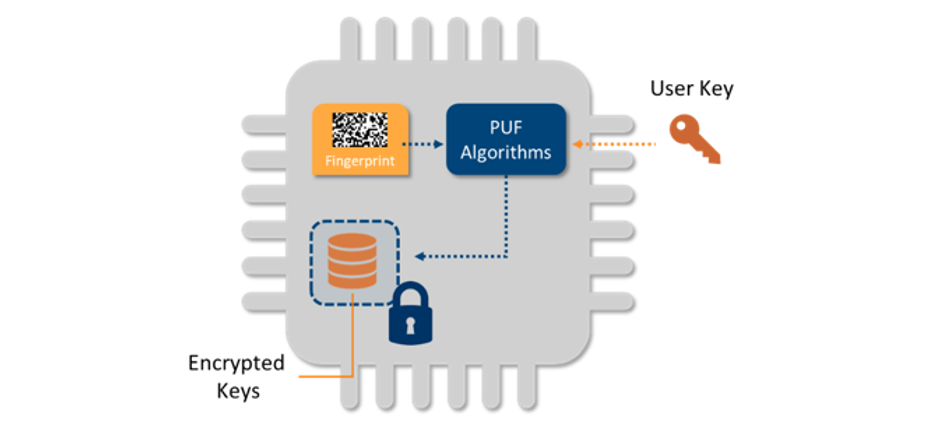
By utilizing these inherent variations, PUFs have been found to be very valuable for use as a unique identifier for any given IC. They do this through circuitry within the IC that converts the tiny variations into a digital pattern of 0’s and 1’s, which is unique for that specific chip and is repeatable over time. This pattern is a “silicon fingerprint,” which is comparable to its human biometric counterpart.
Using certain algorithms, which will be described later in this article, the silicon fingerprint is turned into a cryptographic key that is unique for that individual chip and is used as its root key. This root key is reliably reconstructed from the PUF whenever it is needed by the system, without a need for storing the key in any form of memory. So when the device is powered off, no secret key can be found in any memory; in effect, the root key is “invisible” to attackers, which makes storage of keys with PUFs very secure.
Examples of silicon PUFs include SRAM PUFs, Butterfly PUFs, Buskeeper PUFs, Ring-oscillator PUFs, Arbiter PUFs, Quantum Electronic PUFs, and many more. A few of these examples will be described in more detail later.
The Advantages of Physical Unclonable Functions
Devices, particularly devices that are part of the internet of things (IoT), require keys to protect their data, IP, and operations. These keys can either be provisioned onto the devices by the device manufacturers (also called OEMs) themselves or in an even earlier stage by a chip vendor. When chip vendors supply pre-provisioned chips, they increase the value of the product they are selling to the OEMs. If OEMs decide to do provisioning themselves, they can typically buy chips that cost less.
Regardless of which of the two parties takes on the responsibility of provisioning the cryptographic keys, it is never a trivial task to perform. Injecting secret keys into chips requires a trusted factory, it adds cost and complexity to the manufacturing process, and limits flexibility. This complexity can be avoided by having the keys be created internally inside the chip, either by using an internal random number generator (RNG) or a PUF.
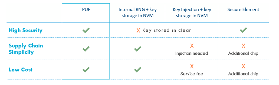
However, generating a key is not the only challenge. This is because storing keys securely on the devices is also far from trivial. Secret keys cannot simply be stored in non-volatile memory (NVM), as NVM is vulnerable to hardware attacks. Hardware attacks that allow adversaries to read NVM content are becoming increasingly more common, making unprotected key storage unviable. Hence, there is a need for alternative secure key storage. One approach would be to add a secure element to the device. However, adding hardware also comes with increasing complexity and cost. A silicon PUF can securely store cryptographic keys without the need to add any additional hardware.
The table below summarizes the security level, supply-chain overhead, and cost of the technology options for provisioning and storing cryptographic keys:
Typical Use Cases for Physical Unclonable Functions in IoT Devices
Key Encryption Key
The best-known use case for PUF technology is creating and storing the cryptographic root key for a device. The cryptographic root key created by the PUF does not require key injection and it cannot be copied from one device to the next. This is because it is never stored, but rather it is reconstructed from the device’s silicon fingerprint every time it is needed. Since this fingerprint is different for every chip, there is no way for an attacker to copy a key from one device to another.
It is a basic cryptographic rule that the same key should never be used for multiple purposes. So, when a device has a security architecture with multiple functions, such as encryption and authentication, every function requires its own dedicated cryptographic key. This means the device requires an anchor of trust that includes key management: the ability to generate and store multiple keys and to manage which key is used for which purpose.
Most PUF implementations allow a device to generate and store a virtually unlimited number of secret keys derived from the PUF root key. All these keys are encrypted with the PUF root key before storage, binding them to the device with no possibility of being copied. External keys that are imported into the device can also be encrypted, or “wrapped,” with the PUF key to enable them to be stored securely. This way the PUF root key serves as a Key Encryption Key (KEK) for a device.
Secure Vault
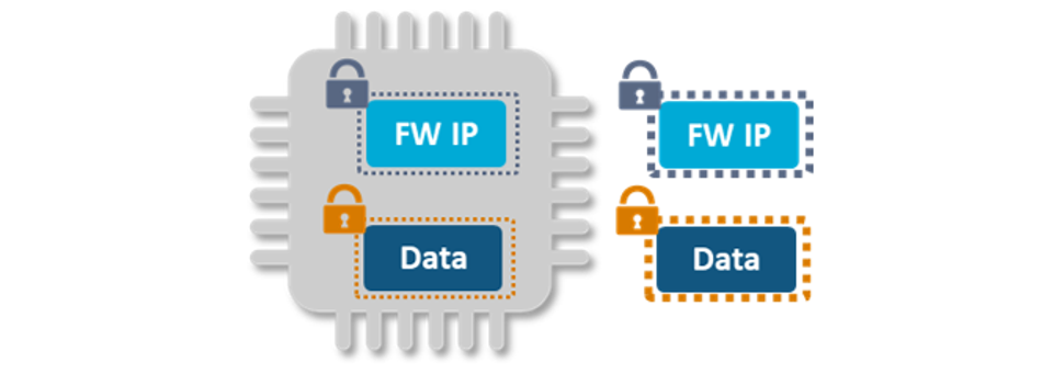
What if an IoT device stores sensitive data that needs to be protected? This could be valuable IP that contains proprietary secrets or measurement data that is privacy sensitive or system critical. That is when the device requires a secure vault. In a secure vault, any data can be stored securely and physically bound to the hardware of the device. This can be achieved easily with a PUF by encrypting all sensitive data with a key derived from the PUF root key. Combining this encryption with message authentication code (MAC) functionality, also enables IP and data to be validated before it is used.
Chip-to-Cloud Authentication
To set up a secure channel between an IoT device and the cloud based on a public key infrastructure (e.g., a transport layer security (TLS) connection with a cloud service), the device and cloud exchange certificates. These certificates authenticate the entities to each other. To produce a certificate for authenticating a device, a public/private key pair is produced from the PUF fingerprint, then authentication is performed through the steps illustrated in the figure below.
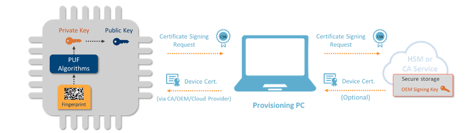
Once the device has obtained a certificate for the public/private keypair, it can start the mutual authentication with the cloud by exchanging certificates. After the mutual authentication, a key agreement protocol is used to exchange cryptographic keys. The exchanged keys are used to apply end-to-end encryption and data authentication. End-to-end encryption ensures attackers cannot eavesdrop on communication between two entities. Data authentication (with hash/MAC functions) assures that received data comes from a trusted source and has not been tampered with in transit.
The private key used to create the device certificate in this scenario is generated and securely stored by the PUF. The session keys devices receive from the cloud during key exchange are also stored securely by encrypting them with keys derived from the PUF.
PUF Processing Algorithms
As stated previously, most PUF implementations require processing algorithms to turn the silicon fingerprint into a cryptographic root key. This is because the silicon fingerprint typically will be slightly noisy between different measurements, as in addition to inate process variations, the electronic properties will also be influenced by ambient conditions, such as temperature and power supply. Hence, a good PUF implementation needs to turn this noisy fingerprint into a fully stable and fully random string of 0’s and 1’s, in order for it to qualify as a cryptographic key. For this purpose most PUF implementations use two processes:
- Error correction, to assure that the derived key is the same every time the PUF is measured
- Privacy amplification, to turn the fingerprint into a fully random string
Error Correction
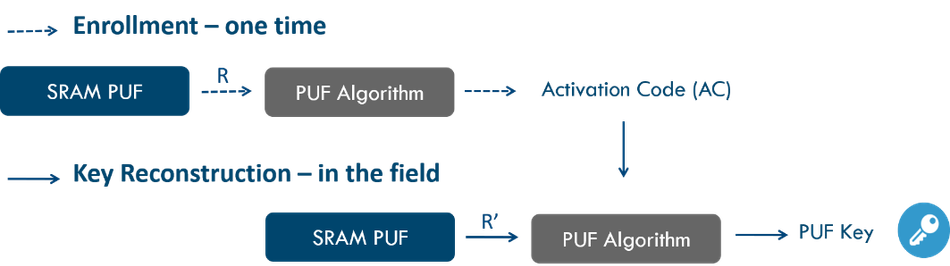
Error correction techniques for cryptographic key reconstruction require an enrollment phase and a reconstruction phase. In the enrollment phase (a one-time process) the PUF response is mapped onto a codeword of an error-correcting code. Information about the mapping is stored in the activation code (AC) or “helper data.” The AC is constructed such that it does not reveal any information about the key. It should be stored in memory that is accessible by the PUF algorithms, but it can be stored off-chip as it is not sensitive. Any change to the AC, malicious or not, will prevent key reconstruction. The AC is only valid for the chip on which it was created.
Each time the device needs the secret PUF key, a new noisy PUF measurement is carried out and the PUF key (without noise) is extracted from the AC and this new PUF response. This is called the reconstruction phase. Both enrollment and reconstruction phases are illustrated below.
Privacy Amplification
Secret keys provide security based on the fact that they are completely random and hence unpredictable. Physical measurements, such as PUF responses, have a high degree of randomness, but are usually not completely uniformly random. Privacy amplification algorithms are used to generate uniformly random keys, for example by hashing a large amount of data with sufficient entropy into a random string of 128 or 256 bits.
What Are the Challenges When Implementing Physical Unclonable Functions?
If PUFs really are such great anchors of trust for devices, why doesn’t every chip vendor and OEM deploy their own PUF implementations? This is because it is not easy to discover and productize new types of PUFs. A lot of research goes into finding elements of a chip that have the type of behavior that is required to create a device fingerprint, at which point the actual productization has not even started yet. Millions of measurements under varying circumstances and with increasing silicon aging are required to define the parameters needed for the error correction and privacy amplification algorithms. The process of productizing a new PUF implementation typically takes years of R&D effort.
And this is not even mentioning the fact that many PUF implementations, even ones that are already known and commercialized today, require significant changes to the hardware of chips. Adding these kinds of PUFs leads to changes in the manufacturing process, either by increasing the number of masks required for production or even requiring non-standard processing steps. This will significantly increase the cost of adding PUF technology to chips, which in turn diminishes the low-cost benefit of using PUFs, as described earlier.
Standard CMOS Implementations of Physical Unclonable Functions
Luckily, these problems can easily be overcome for both chip vendors and OEMs by using standard CMOS implementations of PUFs that can be directly integrated into their devices, without making any changes to the hardware of a chip. The two examples of PUFs that are described below only require IP licensing and can even be deployed on existing hardware. The SRAM PUF targets IoT platforms, such as microcontrollers, where it can be integrated by an OEM as software IP. IoT chip vendors that want to include this PUF in their products can choose between soft- and hardware-IP versions. The Butterfly PUF targets FPGA platforms, typically used for military, government, and aerospace purposes, where it can be implemented in the programmable fabric.
SRAM PUF
The behavior of an SRAM cell depends on the difference of the threshold voltages of its transistors. Even the smallest differences will be amplified and push the SRAM cell into one of two stable states. Its PUF behavior is therefore much more stable than the underlying threshold voltages, making it the most straightforward and most stable way to use transistor threshold voltages to build an identifier.
An SRAM memory consists of a number of SRAM cells. Each SRAM cell consists of two cross-coupled inverters that each are built up by a p- and n-MOS transistor. When power is applied to an SRAM cell, its logical state is determined by the relation between the threshold voltages of the p-MOS transistors in the invertors. The transistor that starts conducting first determines the outcome, a logical ‘0’ or ‘1’.
It turns out that every SRAM cell has its own preferred state every time the SRAM is powered on, resulting from the random differences in the threshold voltages. This preference is independent from the preference of the neighboring cells and independent of the location of the cell on the chip or on the wafer.
Hence an SRAM region yields a unique and random pattern of 0’s and 1’s. This pattern can be called an SRAM fingerprint since it is unique per SRAM and hence per chip. This is why standard SRAM can be used as a PUF, without making any changes to the hardware of a device.
Butterfly PUF
The concept of the Butterfly PUF is based on the idea of creating structures within the FPGA matrix which behave similarly to an SRAM cell during the startup phase. A Butterfly PUF cell is a cross-coupled bi-stable circuit, which can be brought to an unstable state before it settles to one of the two stable states that are possible. The structure consists of two latches whose outputs are cross coupled as indicated in the figure below.
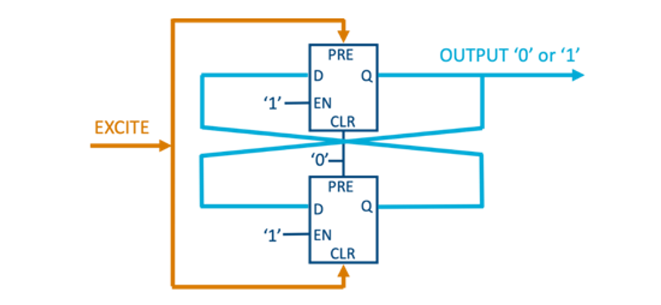
To start the PUF operation, the excite signal is set to high. This brings the Butterfly PUF circuit to an unstable operating point (as both latches have opposite signals on their inputs and outputs). After a few clock cycles the excite signal is set to low. This starts the process of the PUF circuit to attain either one of the two possible stable states, ‘0’ or ‘1’, on the out signal. The stable state depends on the slight differences in the delays of the connecting wires which are designed using symmetrical paths on the FPGA matrix. Hence, these slight variations are based only on the intrinsic characteristics of the integrated circuit and vary from device to device, and position on the FPGA. However, for the same FPGA, latch locations, and routing resources, the stable state tends to be the same over time and over a large temperature range. An attacker cannot derive these stable states from the bitstream (which contains the programming data for the device) since it does not contain these values. Also, an attack cannot derive the stable states from the FPGA itself as these properties are determined by the minute process variations for the basic elements and routing used for the Butterfly PUF structures.
Hence the Butterfly circuit is an implementation of a PUF circuit within the FPGA matrix whose properties depend only on the intrinsic physical characteristics of the integrated circuit and can be used for identification and key generation.
Conclusion
Physical unclonable functions, or PUFs, are a very valuable security building block for chip vendors and OEMs. The cryptographic key that is created and securely “stored” by a PUF provides an anchor of trust for a device. It is the cornerstone of successful use cases for protecting keys, data, IP, and setting up secure connections with the cloud or other devices.
Finding and productizing a PUF in electronic circuitry takes years of R&D effort, but fortunately several PUF implementations are readily available for use. SRAM PUFs and Butterfly PUFs are examples of PUF implementations that require no additional hardware and that are based on standard CMOS processes, which allow them to be integrated into chips and devices at a very low cost. With these silicon proven PUFs, the complexities of key provisioning are resolved for manufacturers, and a strong anchor of trust is readily available for any device.