Building InP-Based Photonic Integrated Circuits with SMART Photonics
Indium phosphide (InP) enables fully integrated photonic chips with high performance and efficiency. As an InP foundry, SMART Photonics supports the transition from design to scalable production through mature platforms and proven design flows.

01 Jun, 2026. 5 minutes read
Introduction
The demand for high-performance integrated photonic systems continues to grow, driven by applications such as AI, datacom, and sensing. These requirements place increasing emphasis on integration, performance, and efficiency at platform level.
Indium phosphide (InP) is widely used in integrated photonics, enabling compact and high-speed systems. To explore how such systems are designed and brought from concept to fabrication, we sat down with Erik Luyk from SMART Photonics for a Q&A session on working with InP-based photonic integrated circuits (PICs). SMART Photonics operates as an independent foundry specializing in InP integrated photonics.
This article is brought to you by PhotonDelta, a foundation focused on accelerating the growth and the maturity of the Integrated Photonics industry Through initiatives such as the Global Photonics Engineering Contest 2026, PhotonDelta creates opportunities for engineers and researchers to translate ideas into real photonic hardware.
Why InP Is the Platform of Choice
Peter (PhotonDelta): What makes InP fundamentally different from other photonic platforms?
Erik (SMART Photonics): InP is the only material that has the physical properties to generate, modulate, and transfer light signals, allowing the integration of all photonic components on a single chip. This way we can make smaller, faster, and energy-efficient chips for our customers.
This capability simplifies system architectures significantly. Instead of combining multiple materials, designers can implement complete integrated photonic systems monolithically. This means fewer constraints when translating a concept into a manufacturable design.
Peter (PhotonDelta): Which applications require InP (not just benefit from it)?
Erik (SMART Photonics): Quite a few, like AI, data & telecom, and structural health monitoring & sensing. But especially datacenters, of course, due to the rapid rise of AI.
In data center environments, the need for high bandwidth and low energy consumption is pushing conventional electronic interconnects to their limits. InP-based PICs provide a path forward by enabling high-speed optical communication with improved efficiency. Similarly, sensing applications benefit from the ability to integrate sources, detectors, and modulation elements on a single platform.
Peter (PhotonDelta): Where does InP deliver the biggest performance gains today?
Erik (SMART Photonics): Full integration of all active and passive components on a chip and therefore efficiency in energy and cost. This level of integration directly impacts system-level performance by reducing losses, improving reliability, and lowering overall system complexity.
For contest participants, this highlights an important design consideration: choosing a platform that aligns with both performance goals and integration requirements.
Designing with InP: From Idea to First Chip
Designing a PIC involves multiple stages, from initial concept to fabrication and testing. While the specifications vary depending on the application, the general workflow reflects a structured approach that is increasingly accessible to a broader range of engineers.
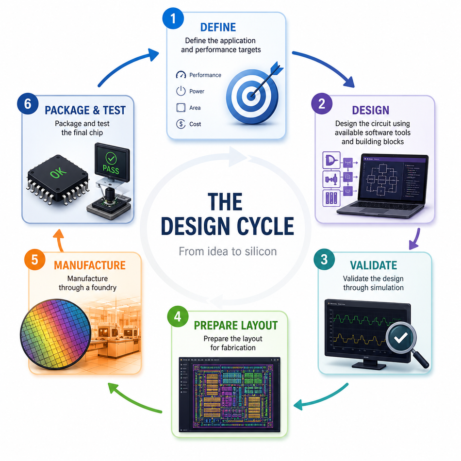
A typical design cycle includes:
Defining the application and performance targets
Designing the circuit using available software tools and building blocks
Validating the design through simulation
Preparing the layout for fabrication
Manufacturing through a foundry
Packaging and testing the final chip
SMART Photonics operates within an ecosystem that includes software providers, design houses, and packaging partners, enabling a collaborative approach to PIC development.
Peter (PhotonDelta): How do your Process Design Kits (PDKs) simplify PIC design?
Erik (SMART Photonics): PDKs provide customers with a set of standardized ‘building blocks’ that perform certain functions on a chip and can be combined in multiple ways, leading to very different functionalities across a broad range of end-user markets. We have 50+ proprietary building blocks in our PDK with 10+ years of experience and knowledge.
When we work with our customers to create photonic chips, we make the process quicker, cost-effective, and more efficient by reusing these proven building blocks, photonic components that have already been tried and tested.
By abstracting the complexity of fabrication, PDKs allow designers to focus on system-level functionality rather than low-level process details. This is particularly valuable for engineers who may not have deep expertise in semiconductor manufacturing but want to develop working integrated photonic systems.
From Prototype to Real-World Deployment
Moving from a prototype to a deployable product introduces additional challenges related to manufacturing, quality, and scalability. This is where the role of a foundry becomes critical.
Peter (PhotonDelta): What changes when moving from prototypes to volume production?
Erik (SMART Photonics): Rather than new breakthroughs, scaling depends on a couple of things: experience, effective feedback loops, and close cooperation across the ecosystem.
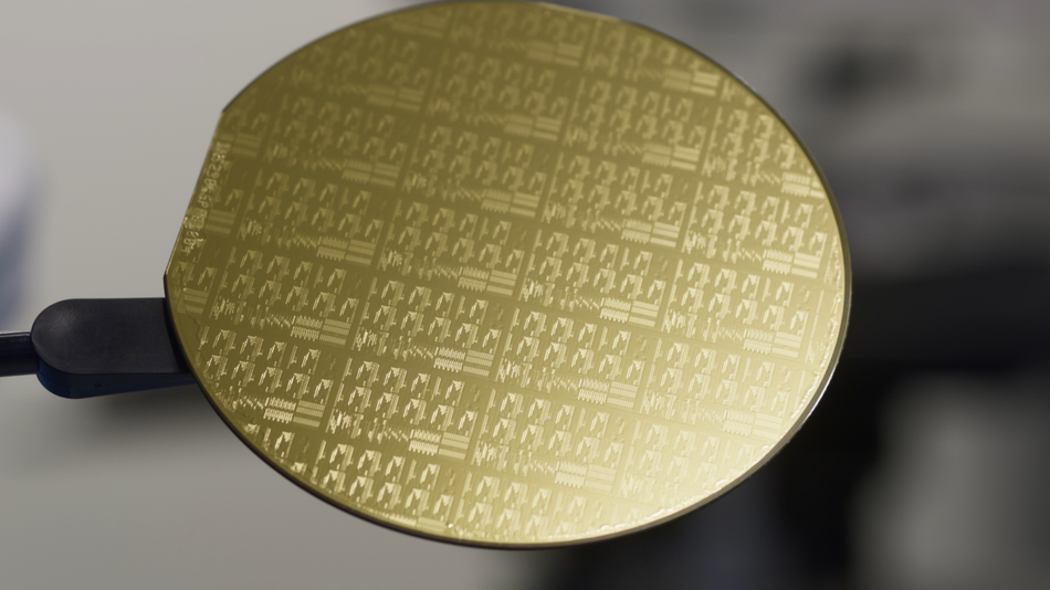
We have the experience and expertise to scale production to larger wafer sizes—from 2-inch to 3-inch, and later from 3-inch to 4-inch. In the near future, we will take the same step towards 6-inch wafers, together with TNO, all while enhancing yield and performance.
On completion in 2028, SMART Photonics’ 6-inch pilot line is expected to produce around 10,000 wafers per year, corresponding to millions of photonic chips.
The pilot line will be hosted by TNO and built at the High Tech Campus Eindhoven. It is part of the EU’s PIXEurope project. It marks an important step towards industrial-scale production – and shows how scaling is not driven by technology alone, but by the experience, feedback loops and ecosystem cooperation behind it.
Peter (PhotonDelta): How do you ensure consistency and quality?
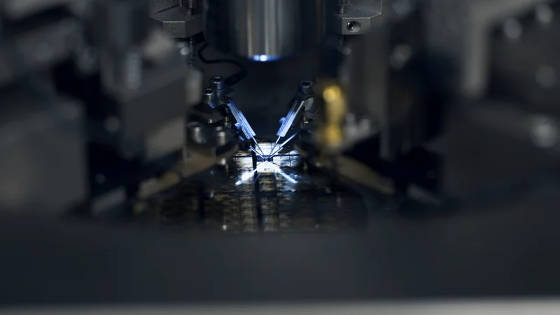
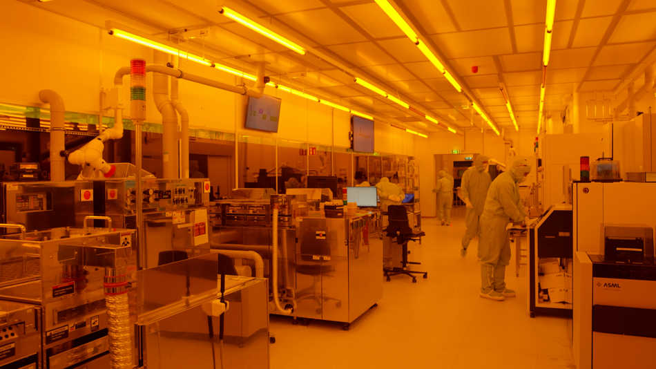
Erik (SMART Photonics): Producing a wafer with photonic chips requires a series of about 450 complex steps. Ramping up production means optimising each of these steps. The challenge of ensuring all chips on a wafer function flawless becomes greater as the wafer size increases. A lot hinges on finding the right settings.
When depositing plasma on a wafer as part of the lithography process, for instance, a specific voltage is applied to the wafer. This voltage determines the speed with which molecules are pulled to the wafer to create a layer of plasma. The challenge is to find the optimal voltage level. Spreading the layer equally over the wafer is another challenge. One needs a keen sense of touch for that, something our engineers gathered over the years.
Peter (PhotonDelta): What role does a pure-play foundry model play here?
Erik (SMART Photonics): As an independent foundry, SMART Photonics focuses on manufacturing photonic components and integrated circuits for its customers. This model allows customers to retain their intellectual property while leveraging shared infrastructure and expertise.
A mature platform with proven processes and building blocks reduces the number of design iterations required and enables faster transition from concept to production.
In addition, scaling capabilities are continuously evolving. Currently, SMART Photonics produces on 4-inch wafers (max capacity 5000 wafers) and is expanding to 6-inch wafer production in collaboration with TNO, with a pilot line expected to be finalized around the end of 2027.
For early-stage designs emerging from events like the Global Photonics Engineering Contest, this kind of infrastructure provides a pathway from prototyping to eventual scaling.
Together we can bring your innovation to life!
Conclusion
InP continues to play a critical role in advancing integrated photonics, offering the ability to generate, modulate, and transfer light signals within a single platform. This capability enables the development of compact, high-performance, and energy-efficient integrated photonic systems across applications ranging from AI-driven data centers to sensing.
Foundries such as SMART Photonics occupy a key position in this ecosystem, supporting the transition from design to fabrication and ultimately to scalable production.
Initiatives like the Global Photonics Engineering Contest 2026 are lowering the barrier for engineers to engage with these technologies. By providing a platform to develop and test ideas, such efforts are helping bring new innovations closer to reality.
As access to advanced photonic platforms continues to expand, the combination of design ecosystems, foundry capabilities, and global initiatives is expected to play an important role in shaping the next generation of photonic systems.