Aluminum Oxide Photonic Integrated Circuits: Insights from Aluvia Photonics
Aluminum oxide PICs are gaining attention for their broad wavelength coverage, low optical losses, and support for on-chip optical amplification. In this discussion, Steve Stoffels, the CEO of Aluvia Photonics, explains where the platform fits and how teams can design with it.

29 Jul, 2026. 7 minutes read
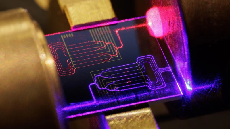
As integrated photonics expands into quantum systems, UV sensing, LiDAR, optical communications, and advanced spectroscopy, existing photonic integrated circuit (PIC) platforms are running into material limitations.
Silicon photonics and silicon nitride, while widely adopted, are non-transparent below roughly 400 nm, restricting their use in ultraviolet and several quantum applications. Indium phosphide supports active optical functionality but comes with higher fabrication complexity. In many cases, system developers are forced to combine multiple material platforms to achieve the required optical performance, increasing cost, packaging complexity, and integration overhead.
These challenges are also relevant for teams participating in the Global Photonics Engineering Contest 2026, where application requirements often extend beyond the limits of certain PIC platforms.
Aluminum Oxide (AlOx): A Platform Built for the Full Spectrum
Aluminum oxide (AlOx) is emerging as an alternative platform designed to address these gaps. The material offers one of the broadest optical transparency windows in integrated photonics, spanning from approximately 200 nm in the ultraviolet to 3 μm in the mid-infrared. It also supports ultra-low propagation losses, high optical power handling, and rare-earth doping for on-chip optical amplification, capabilities not simultaneously available in conventional silicon-based photonic platforms. In addition, AlOx remains compatible with CMOS manufacturing workflows and scalable wafer processing.
Aluvia, a leading AlOx PIC manufacturer, offers a unique platform spanning UV to mid-infrared wavelengths. Through Multi-Project Wafer (MPW) runs, a Luceda-based Process Design Kit (PDK), and dedicated wafer production, Aluvia makes AlOx more accessible. In the following discussion, Steve Stoffels, the CEO of Aluvia, shares how AlOx compares to existing PIC platforms and where it fits best.

Peter (PhotonDelta): Aluvia specializes in AlOx-based PICs. What differentiates the platform technically, and which application domains benefit most from its properties?
Steve (Aluvia): Aluminum oxide stands apart from other photonic platforms through a combination of properties that no single competing material can fully replicate. Its optical transparency window spans from 200 nm in the ultraviolet all the way to approximately 3 μm in the mid-infrared, a range that exceeds what silicon photonics, silicon nitride, or indium phosphide individually offer. This is paired with exceptionally low propagation losses: around 5 dB/m at 1550 nm in the near-infrared and approximately 1 dB/cm at 369 nm in the UV.
AlOx also handles optical power significantly better than silicon nitride, up to an order of magnitude higher, and exhibits superior linearity. Critically, AlOx is amenable to rare-earth doping, particularly with Erbium (Er³⁺), which enables on-chip optical amplification. This is a capability that silicon-based platforms cannot offer, and it opens up a category of applications like integrated optical amplifiers and active photonic circuits that are structurally inaccessible to other passive platforms.
The application domains that benefit most include:
Optical communications, where on-chip Erbium-doped waveguide amplifiers (EDWAs) can replace bulky fiber amplifiers
Quantum technologies, where UV transparency is essential for ion and atom trapping at the heart of next-generation optical clocks and quantum computers
LiDAR systems, where high power handling enables compact solid-state beam steering
Augmented reality, where efficient transmission in the blue wavelength range is critical for high-brightness display engines
Integrated UV lasers for spectroscopy, biomedical applications, and advanced manufacturing.
Peter (PhotonDelta): Tell us something about your products and services. How do your building blocks and product modules integrate with customer-specific architectures? Are they intended as drop-in solutions or as starting points for customization?
Steve (Aluvia): Aluvia offers a layered product portfolio designed to take teams from early-stage R&D through volume manufacturing without forcing re-architecture at each step. Our MPW program allows teams to prototype cost-effectively through shared wafer runs, with quarterly cadence and two passive AlOx stack options: 100 nm for UV-visible applications and 400 nm for near-infrared. Design areas of 5×10 mm² or 10×10 mm² make the program accessible to research groups, startups, and university teams.
For teams moving toward production, Dedicated Wafer Runs offer full-volume fabrication with stack-level customization, including active, rare-earth-doped AlOx layers, on both 100 mm and 200 mm wafer platforms. Our PDK, available through the Luceda Photonics Design Platform, gives designers a familiar and well-supported environment for working with AlOx from day one.
Peter (PhotonDelta): What are the key volume applications of AlOx? Where do you see the strongest commercial momentum for AlOx photonics over the next few years?
Steve (Aluvia): Near-term volume opportunities are concentrated in optical communications and quantum technologies.
In communications, demand for integrated on-chip amplification is accelerating as AI-scale datacenters push the limits of conventional optical interconnects and their amplification solutions. AlOx-based EDWAs offer gain in the C-band in a fully integrated, wafer-scale format. We see strong commercial pull from the high-performance networking and datacenter connectivity segments, where power efficiency and miniaturization are rapidly becoming as important as raw throughput.
In quantum technologies, AlOx’s UV transparency gives it a structural advantage for ion trap and atom trap photonics, a segment growing rapidly as quantum computing and sensing hardware matures from laboratory demonstrations toward deployable systems.
LiDAR for mobility, robotics, and environmental sensing represents a third strong vector, where AlOx’s power handling enables the compact solid-state architectures next-generation systems require. Further out, augmented reality optics and chip-integrated UV lasers for spectroscopy and biomedical applications represent emerging markets that AlOx is uniquely positioned to serve.
Peter (PhotonDelta): Could you share any recent or upcoming projects that Aluvia is working on?
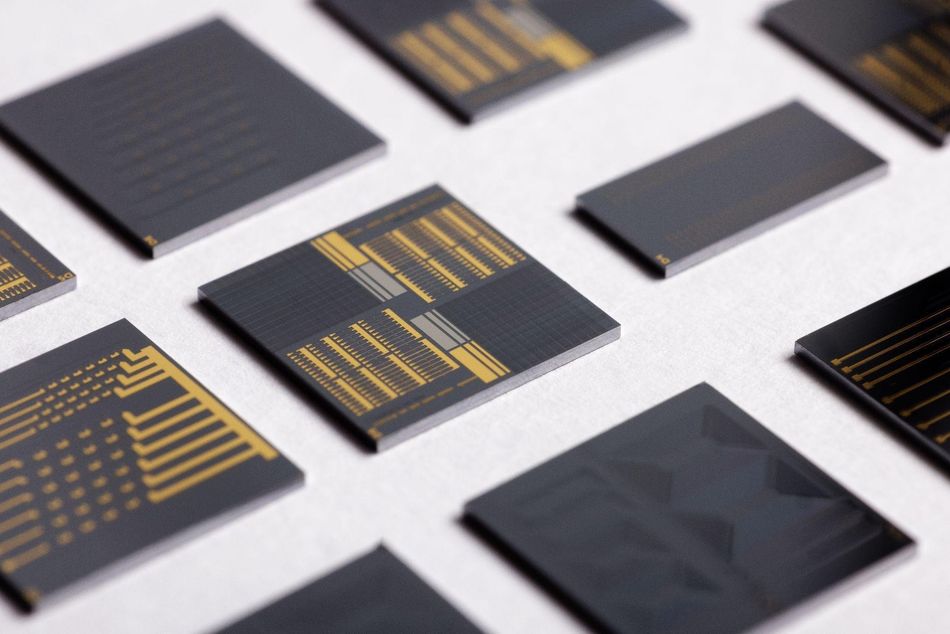
Steve (Aluvia): Our project portfolio reflects both the breadth of the AlOx platform and the growing European commitment to deep-tech integrated photonic infrastructure.
Extended cavity UV laser, Nature Communications (2025), published in November 2025, is a landmark paper from the University of Twente that demonstrated the first integrated, extended cavity diode laser built entirely from UV-transparent materials, combining AlOx waveguide circuits with gallium nitride amplifiers.
The laser achieves milliwatt-level on-chip output power in the violet range (403–408 nm), a record-low intrinsic linewidth of around 300 kHz, and better than 43 dB side-mode suppression. Critically, it tunes mode-hop-free to atomic transition frequencies, such as the strontium transition, which is precisely what portable optical clocks and ion-based quantum computers require. This result validates AlOx as the enabling material for a new class of UV-integrated lasers and directly underpins Aluvia’s quantum-facing product roadmap.
P4Q, Photonics for Quantum: Aluvia is a partner in P4Q, a €50 million European quantum pilot line coordinated by the University of Twente and co-funded by the EU’s Chips Joint Undertaking and twelve national governments. P4Q bridges the gap between laboratory quantum photonics and industrial manufacturing, developing process and assembly design kits across multiple platforms, with AlOx as a key pillar. For Aluvia, P4Q is a critical step toward positioning AlOx as a production-ready platform for the quantum industry, embedded within a structured European supply chain.
femto-i-Comb, EIC Transition: Building on the European Innovation Council (EIC) Pathfinder project FEMTOCHIP, femto-i-Comb aims to deliver the world’s first fully stabilized, integrated femtosecond laser-based frequency comb. By combining on-chip continuum generation and carrier-envelope locking, the project creates ultra-stable optical and microwave sources for applications spanning high-resolution environmental and health sensing, LiDAR, RADAR, and next-generation signal generation. Aluvia contributes its AlOx waveguide platform alongside partners including DESY, LIGENTEC, and Cycle Lasers.
Qu-PIC, Horizon Europe RIA: The Quantum Universal PIC platform project has selected AlOx as its backbone technology for its low propagation losses and spectral coverage. Qu-PIC targets a comprehensive quantum PIC building block library: tunable lasers at 399 nm, 411 nm, and 935 nm; UVC external cavity lasers at 280 nm; squeezed photon sources; and single-photon detectors. Two demonstrators are in development, a source of GKP states for quantum processing and a ytterbium-ion-based atomic clock, all within a framework explicitly aimed at securing European quantum photonic supply chain sovereignty.
PHANTOM, Photonic Gas Sensing: PHANTOM applies AlOx photonics to accurate identification and concentration measurement of gases for safety, sustainability, and efficiency. Target applications include detecting toxic hydrogen cyanide during manure storage, monitoring ammonia leaks in combustion engines and hydrogen fuel cells, and tracking ethylene in fruit storage facilities. Gas detection is achieved through laser absorption spectroscopy, where AlOx’s broad spectral window and ultra-low-loss waveguides are decisive advantages. The consortium, including OnePlanet Research, Radboud University, Bronkhorst, Epiphany, and Sensor Sense, kicked off in December 2025.
Peter (PhotonDelta): If a team is considering an AlOx-based design, what technical constraints should they carefully evaluate?
Steve (Aluvia): Aluvia’s AlOx technology provides a powerful and versatile platform for integrated photonics, but teams should approach it with a clear-eyed understanding of where it fits and what to plan around. The most important upfront decision is wavelength range. AlOx stacks are optimized for specific spectral windows. Our 100 nm layer targets UV-visible applications, while the 400 nm layer is designed for near-infrared. Selecting the right stack at the outset is essential: switching later means a new design and a new fabrication run, with both time and cost implications.
Early-stage clarity on the target wavelength and integration architecture is therefore critical to fully take advantage of AlOx’s strengths. AlOx is an advanced photonic platform particularly well suited to low-loss light guiding, splitting, filtering and on-chip optical amplification across a broad wavelength range. For applications that also require high-speed electro-optic modulation or electronic integration, AlOx can be combined with complementary technologies through a hybrid integration approach. Planning this architecture from the outset allows each material platform to be used where it delivers the greatest performance, while avoiding the compromises that can arise when all functions are forced into a single material system.
Peter (PhotonDelta): How can participants in the PhotonDelta Global Photonics Engineering Contest 2026 leverage Aluvia’s platform and design ecosystem?
Steve (Aluvia): Aluvia is an industry partner in the Global Photonics Engineering Contest 2026. Our MPW program is the natural entry point for contest teams: affordable, rapid prototyping through shared wafer runs with no commitment to a fully dedicated wafer at the concept stage. The Luceda PDK provides a structured starting environment, and our team is available to support from early design through tape-out.
The AlOx platform suits the contest’s core application domains, offering capabilities unavailable on conventional platforms. We encourage teams to reach out early to discuss whether AlOx is the right fit. Aluvia’s role as an ecosystem partner means the winning team has a credible, supported path from concept to fabricated chip.
Advancing Innovation in Integrated Photonics with AlOx
The PhotonDelta Global Photonics Engineering Contest 2026 is a real opportunity, not just visibility. With a network of industry partners ready to help turn a concept into a working device, what might seem ambitious becomes achievable. The path runs from idea to platform to fabrication to application. With the AlOx ecosystem in place and Aluvia as a partner, the support to walk that path is already there.