Sustainable electronics: Mass manufacture mulit-layer FPCBs and RPCBs with inkjet printing
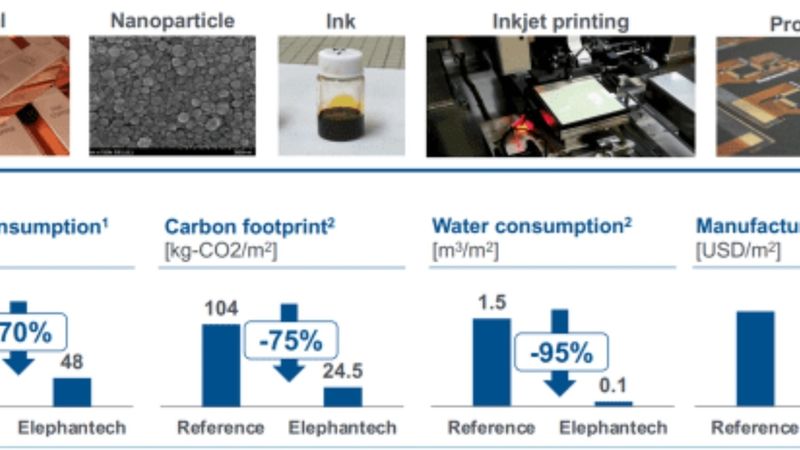
Additive electronics is sustainable reduceing copper and water consumption vs. the traditional PCB production processes by 70% and 95%, respectively whilst reducing the carbon footprint by 75%. Here you will read about the latest advances by one of the leading firms in the field from Japan
19 Jun, 2023. 4 minutes read
Elephantech is developing mass production of multi-layer flexible and rigid PCBs [FPCBs and RPCBs] using inkjet printing. This is an important industry development which enables more sustainable electronic production. This article appeared here on TechBlick.com first.
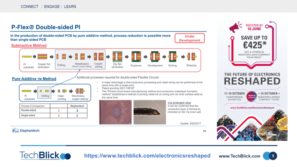
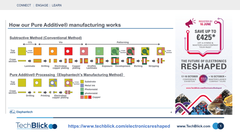
Slide [1] compares the convention process vs the inkjet printed process, showing how the number of production steps and the amount of material consumed can be reduced since ink-printing enables additive (vs subtractive) manufacture.
Note in slide [1] how Elephantech is also developing technology to enable double-sided FPCBs with drilled vias[more on this later]
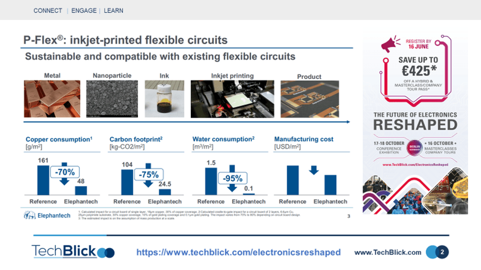
Slide [2] shows how Elephantech is a vertically integrated operation now, covering material development [copper nanoparticles] to ink formulation to inkjet printer development to production of FPCBs in house. The ultimate goal is to be an equipment supplier. However, they will do manufacturing to gain production experience to perfect the process and machinery in the years to come
Slide [2] also demonstrated the sustainability of the process, showing that the additive inkjet based process reduces copper and water consumption vs. the traditional etched process by 70% and 95%, respectively whilst reducing the carbon footprint by 75%. These are very important achievements, in particular considering how all major electronics OEMs are now pushing for greener value chains [10% of the CO2 footprint of Apple comes from PCB production!]
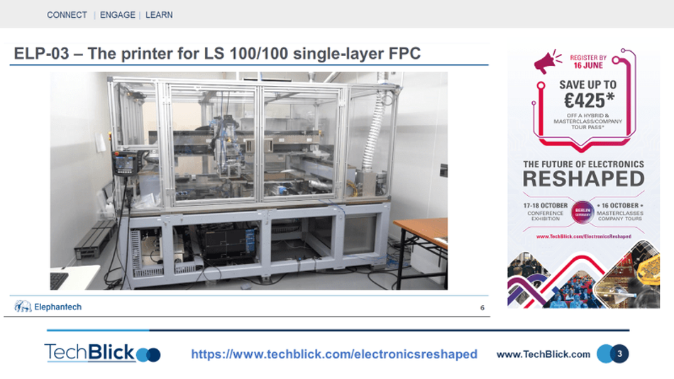
Slide [3] shows an inkjet printer under development. This is not the final design and many design questions remain open such as number of print heads or the exact choice of piezo-actuated printer suppliers.
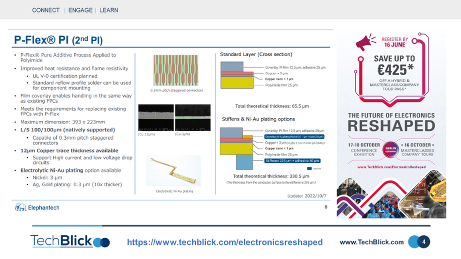
Slide [4] shows the current achievements. Incredibly, they can directly achieve inkjet printed linewidth-to-spacing [L/S] ratio of 100/100um without the need for any laser ablation or laser finetuning. This is an important achievement which is the result of high optimization between inkjet head, control system, and ink and substrate development.
In this process, first a copper nanoparticle ink [50-100 nm particles] is inkjet printed. The Cu nanoparticle solution is specially formulated with surface functionalization [my guess is the substrate PI is also somehow pre-treated] to promote strong adhesion to the surface. The inkjet printed Cu layers are then photosintered using a Xenon or similar lamp.
The idea of the activation here is not to achieve high conductivity but to achieve a solid network of deposited copper nanoparticles with strong substrate adhesion which acts as a seed layer. In fact, conductivity is not measured. This is because the formulation of these Cu nanoinks must fulfill different criteria as those aimed at printed electronics.
In the recent past, Ag seed layers were used. This important transition is motivated by cost savings.
The seed layer is then thickened using electroless plating. Plated copper gives bulk level conductivity and solderability, making it [unlike circuits with printed paste] a drop-in replacement performance-wise
As shown in slide [4], a 12um thick copper plated can be achieved. This is a significant advancement vs. the previous achievement of 3um. Importantly, the adhesion remains strong even with a thick plated layer
Slide [5] shows how double sided FPCBs can be achieved. Here, a via is drilled into the PI substrate and is then metallized with inkjet printing before being plated.
Slide [6] shows the future roadmap. Firstly, the deposited layer will be thickened to 30um to support more PCB options. This needs much better adhesion and must have more optimized interplay between functionalized Cu nanoparticles, substrate surface, and electroless plating process. Next, they will transition from flexible to rigid PCBs and add more layers to the capabilities.
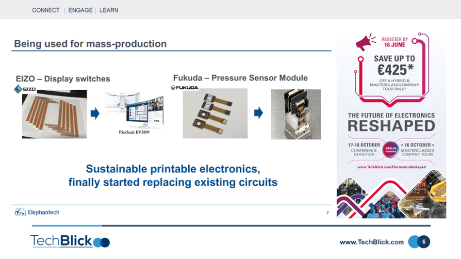
These developments will take time and are an engineering challenge, but in the end this is a more sustainable production process yielding high performance PCBs compared to etched PCB production. As such, in the long term, it will have its role in the industry without doubt. Indeed, as shown in slide [7] it is already on the market.