MOSFET Switch: How to Use a MOSFET as a Switch
Learn how to use MOSFETs as switches, explore circuit configurations, and optimize performance for efficient, reliable electronic designs.

27 Oct, 2026. 18 minutes read
This article was first published on
www.unikeyic.comA MOSFET switch turns a load on and off with a small control voltage. There are no moving parts and no contacts to wear out. You need a gate signal and a low-resistance path between drain and source.
Although the basic concept is simple, many first attempts fail because the MOSFET is not driven, protected, or thermally managed correctly. The MOSFET stays half on. The gate floats. The part runs hot, or a relay coil kills it with a voltage spike.
This guide shows how to use a MOSFET as a switch the right way. You will build a basic N-channel low-side circuit and set up the gate network. You will also protect the device on inductive loads. Then you will pick a part, check its heat, and troubleshoot common faults. It covers enhancement-mode power MOSFETs switching DC loads.
What Is a MOSFET Switch and How Does It Work?
The same switching principle applies, but the required gate-to-source polarity depends on whether the device is N-channel or P-channel. A power MOSFET can act as an electronic switch when its gate-to-source voltage places the drain-source path either in cutoff or in a low-resistance on-state. For an enhancement-mode N-channel MOSFET, a sufficiently positive VGS enhances the channel. For a P-channel MOSFET, the required gate-to-source polarity is reversed. In either case, the applied VGS must be checked against the conditions under which RDS(on) is specified in the datasheet.
We focus on enhancement-mode power MOSFETs, which remain off at zero gate-source voltage. The illustration below shows an N-channel device, while a P-channel device requires the opposite gate-to-source polarity. The underlying terminals, channel formation and operating regions are explained in our MOSFET fundamentals article.
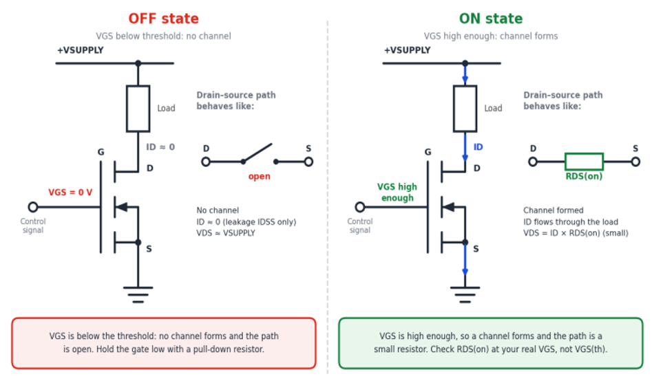
| VGS | Drain-source path | State |
|---|---|---|
| VGS at the required OFF-state level (typically 0 V) | Open (tiny leakage) | OFF |
| VGS with the required polarity and magnitude, per datasheet | Low resistance (RDS(on)) | ON |
MOSFET OFF State: Cutoff and Leakage
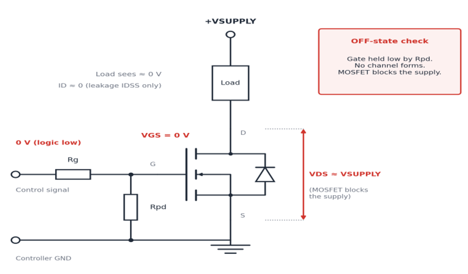
When VGS does not have the polarity and magnitude required to turn the MOSFET on, the device is in the cutoff state. For an enhancement-mode MOSFET, no normal conducting channel is formed, so the drain-source path has very high resistance and the MOSFET blocks most of the current. A small leakage current can still flow.
The drain-source leakage current at zero gate voltage is often listed as IDSS in the datasheet. The specified value depends on the test conditions, including VDS and temperature. It is usually very small, but it can matter in low-power or battery-powered designs. Leakage current can also increase as the MOSFET gets hotter, so check the datasheet under your expected operating conditions.
The gate needs special attention. Because the gate is insulated, it has very little DC current flow. If the gate is left floating, it can hold unwanted charge or pick up electrical noise from nearby wires or other parts of the circuit. This can cause the MOSFET to turn on, turn off, or partially turn on when you do not want it to.
For reliable switching, always give the gate a defined voltage. Do not leave it floating. A resistor is commonly used to pull the gate to the required off-state voltage, as shown in the circuit section below.
MOSFET ON State: Low RDS(on), Not "Zero Resistance"
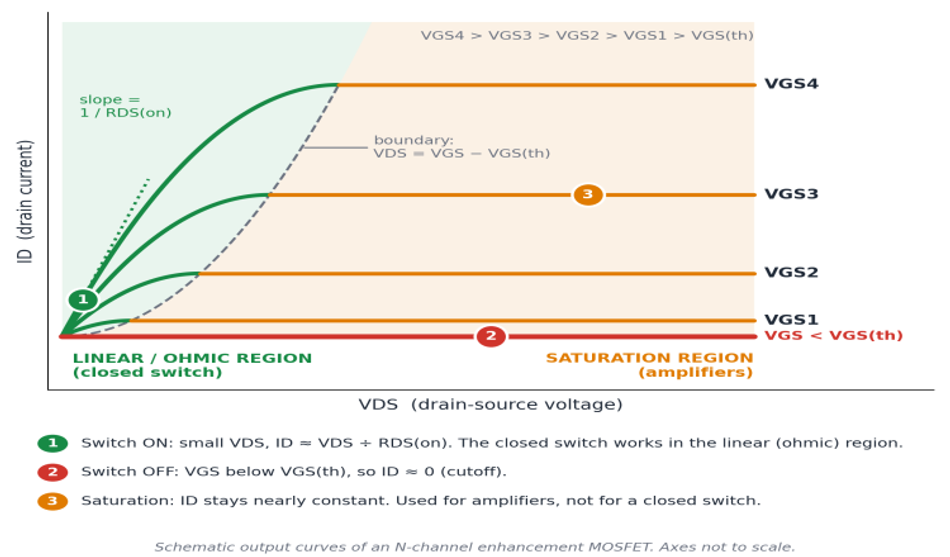
When VGS is high enough, a conducting channel forms in an N-channel enhancement MOSFET. Current can then flow between the drain and source. When a power MOSFET is used as an ON switch, it normally operates with a low VDS and low resistance. This is called the ohmic or triode region. This region is sometimes incorrectly called the saturation region. In MOSFET operation, saturation is a different region where the drain current becomes much less dependent on VDS. It is commonly used in amplifier and other analog circuits, rather than as the low-resistance ON state of a switch.
When the MOSFET is ON, it behaves like a small resistance called RDS(on). The voltage drop across it is approximately ID × RDS(on). This resistance is not zero and usually increases as the MOSFET gets hotter. RDS(on) also depends on the gate-source voltage. A higher VGS can reduce RDS(on), but only within the device's specified range. This is why the RDS(on) value listed in a datasheet, often measured at 10 V, may be different from the value in your actual circuit.
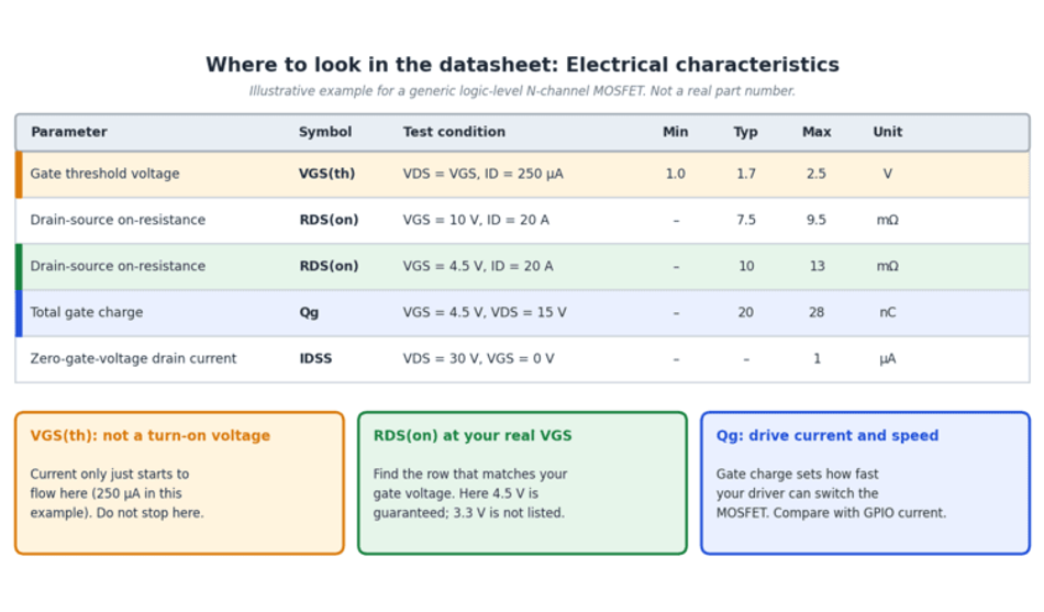
A common mistake is treating VGS(th) as the voltage needed to fully turn on a MOSFET. It is not. VGS(th) is the gate-source voltage at which the MOSFET just begins to conduct a small drain current under the datasheet's test conditions. To turn the MOSFET on properly and achieve low RDS(on), you usually need a higher VGS.
| Wrong judgment | Correct judgment |
|---|---|
| "VGS is above VGS(th), so it is fully on." | "The datasheet guarantees this RDS(on) at my actual VGS, so it is on." |
Judge the ON state by the guaranteed RDS(on) at your real gate voltage. We do the power math later.
Basic N-channel MOSFET Switch Circuit
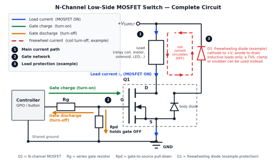
The N-channel low-side switch is the usual starting point. It is the simplest N-channel MOSFET switch to build. In this NMOS switch, the source connects to the low side of the system, often ground. The load sits between the positive supply and the drain. The control signal drives the gate.
When the gate goes high, current flows through the load and down to ground. When the gate goes low, the current stops. We build it in three parts: the main current path, the gate network, and load protection.
Connect the MOSFET and Load in a Low-Side Configuration
This N-channel MOSFET circuit has one main current path. Current leaves the supply, passes through the load, enters the drain, and leaves through the source to ground. The MOSFET therefore needs a drain-source current rating appropriate for the load and its transient conditions.
Wire it in this order:
Connect the source to the negative rail (ground).
Connect the drain to one side of the load.
Connect the other side of the load to the positive supply.
Connect the gate to your control signal through the gate network.
Join the controller ground to the power ground.
Step five is easy to forget. VGS is measured between gate and source. Without a shared ground, the gate voltage has no reference. The MOSFET will behave strangely.
Also note the body diode. Most standard discrete silicon power MOSFETs include an intrinsic body diode. In an N-channel MOSFET, the body diode has its anode at the source and its cathode at the drain. It is normally reverse-biased in a correctly connected low-side switch, but it can conduct during reverse-current or transient conditions.
This is a low-side design because the switch sits between the load and ground.
Pin order differs between packages, so confirm which leg is the gate, drain, and source in the datasheet before you solder. Before you power up, trace the loop once on paper: supply, load, drain, source, ground. If any link in that chain is missing, the load will not switch.
Add a Gate Resistor and Gate-to-Source Pull-Down Resistor
Two resistors around the gate solve two different problems.
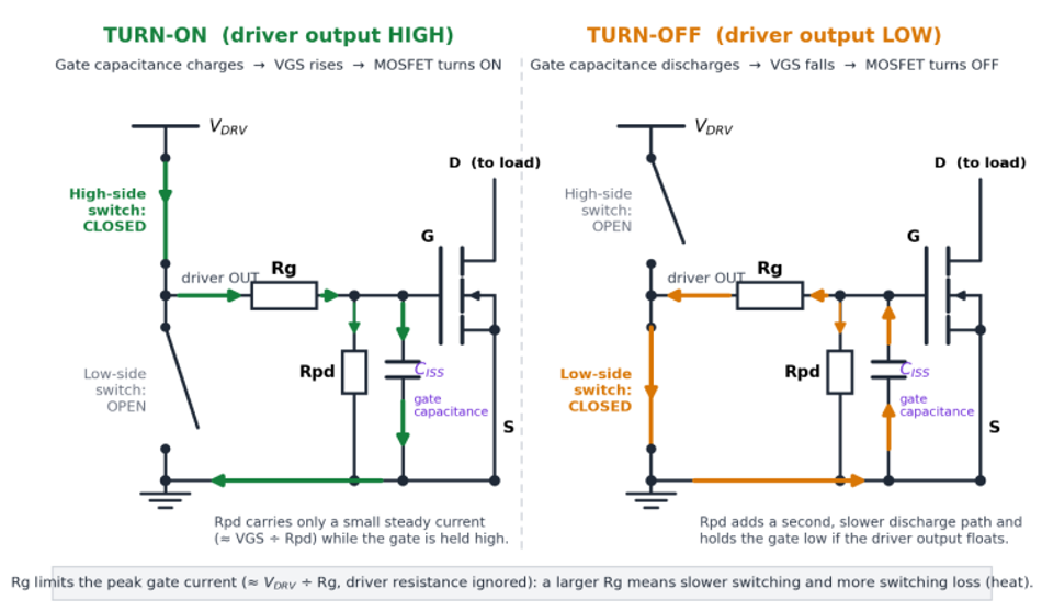
The series gate resistor sits between the driver and the gate. It limits peak gate current during gate charging and discharging, controls switching speed, and helps damp ringing. The actual peak current depends on the total gate-drive path resistance, including the driver's output resistance, the external gate resistor, and the MOSFET's internal gate resistance.
The gate-to-source pull-down resistor sits from gate to source. It holds the gate low during startup, reset, or when the controller pin is high-impedance. Many microcontroller pins float during boot. Without a pull-down, the load can fire on its own.
How much the pull-down matters depends on the driver. A push-pull output that is always driven high or low holds the gate firmly. A pin that goes high-impedance, or a switch that can only pull high, needs the pull-down to turn the MOSFET off.
These two resistors do different jobs, so one cannot replace the other. Neither resistor is used to limit the load current.
| Resistor | Location | Job |
|---|---|---|
| Series gate resistor | Driver to gate | Limits peak gate current, controls switching speed, reduces ringing |
| Gate-to-source pull-down | Gate to source | Keeps the MOSFET off by default |
| Load current-limiting resistor | In series with load | Sets load current, unrelated to the gate |
For an LED load, size the resistor as R = (VSUPPLY − VF − VDS(on)) ÷ ILED. Do not copy a value from a forum post. It depends on your supply and LED.
A button, sensor, or GPIO pin can act as the trigger. People often call this a MOSFET trigger switch. The trigger only changes the gate voltage. The gate network decides what happens in between.
These values are only starting points and change with the MOSFET, the driver, and the load. Small logic-driven circuits often use tens to a few hundred ohms in series and 10 kΩ to 100 kΩ for the pull-down. Check gate charge and switching speed before you commit. A bigger series resistor slows switching and adds heat. For more, read our gate resistor selection guide.
Protect the MOSFET When Switching an Inductive Load
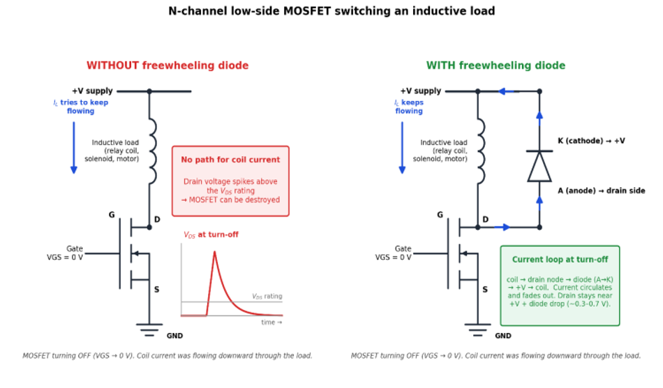
Relay coils, solenoid valves, and motors store energy in their magnetic fields. Their current cannot stop instantly. When the MOSFET turns off, the stored energy can cause the drain voltage to rise sharply. If this voltage exceeds the MOSFET's maximum VDS rating, the device can be damaged.
Inductive loads such as relays, solenoids, motors, and valves require a suitable path for stored inductive energy when the MOSFET turns off. Depending on the required release speed and voltage limit, this may be a flyback diode, a TVS or Zener clamp, a snubber, an active clamp, or protection integrated into the driver.
Choose a diode with suitable current and reverse-voltage ratings. Schottky, fast-recovery, and standard rectifier diodes can be used depending on the application. Keep the diode close to the load and use short connections. A simple diode makes the coil current decay more slowly, so a relay or solenoid may release slightly later.
Resistive loads such as heaters and LED strips normally do not need inductive-energy protection. Inductive loads such as coils, motors, and solenoid valves require a suitable protection method that meets the circuit voltage limit and release-time requirements.
TVS diodes, Zener clamps, RC snubbers, active clamps, or protection integrated into the driver may be useful when faster turn-off or tighter voltage control is needed.
Low-Side vs. High-Side MOSFET Switching
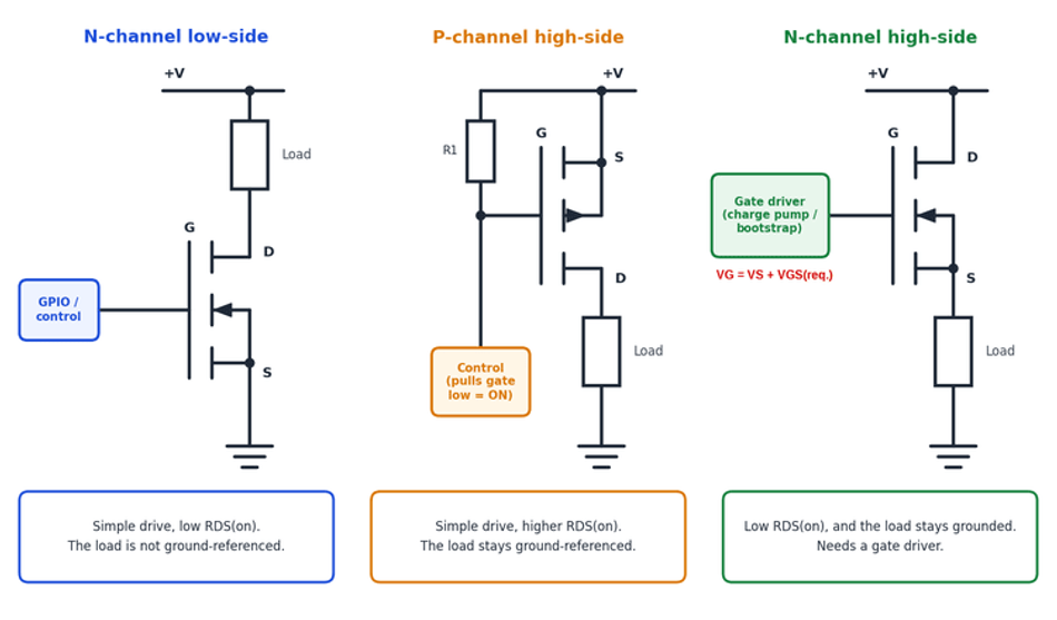
High-side and low-side describe where the MOSFET is placed relative to the load; they are not fixed MOSFET types. The choice between N-channel and P-channel MOSFETs affects gate-drive complexity, conduction loss and the most suitable switch position. A low-side switch is placed between the load and ground, while a high-side switch is placed between the power supply and the load.
Use a high-side switch when the load needs to remain connected to ground. The trade-off is usually between gate-drive complexity and switching performance. High-side and low-side are the two common ways to place a MOSFET switch around a load. The table below compares these common arrangements.
| Topology | Gate drive | Strength | Limit |
|---|---|---|---|
| N-channel low-side | Simple | Low RDS(on), easy drive | Load is not ground-referenced |
| P-channel high-side | Fairly simple | Easy high-side control | Higher RDS(on) for the same size |
| N-channel high-side | Needs a driver | Low conduction loss | More parts |
P-channel MOSFET as a High-Side Switch
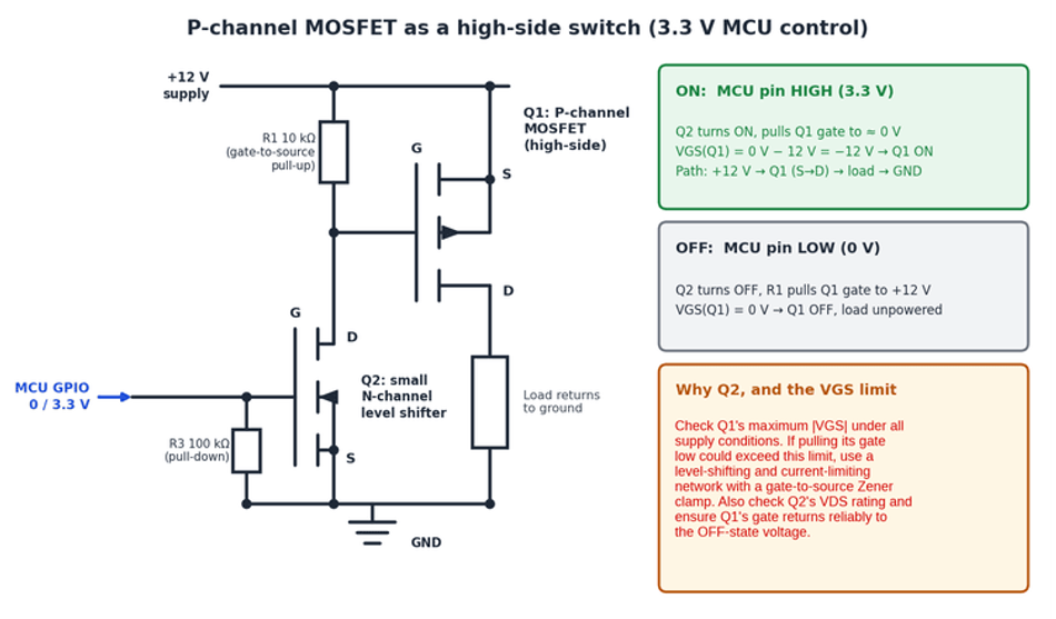
A P-channel MOSFET is often suitable for relatively simple high-side switching applications. Connect the source to the positive supply. Connect the drain to the load. The load's other side goes to ground.
A P-channel MOSFET switch circuit turns on when the gate is pulled below the source. On a 12 V supply, a gate at 0 V gives VGS of −12 V. That turns it on. Return the gate to the source voltage, and it turns off. A resistor from gate to source keeps it off by default.
| Gate voltage (relative to source) | State |
|---|---|
| VGS = 0 V | OFF |
| Sufficiently negative VGS | ON |
Check the MOSFET's maximum |VGS| rating under all supply conditions. If pulling the gate low could exceed this limit, use an appropriate level-shifting and current-limiting network together with a gate-to-source Zener clamp. Also verify the VDS rating of the small pull-down transistor and ensure that the PMOS gate can still return reliably to the off state.
A 3.3 V microcontroller cannot pull the gate up to a 12 V source to turn the device off. A small N-channel MOSFET is often used as a level shifter for this. In the circuit below, Q2 is that level shifter. R1 holds Q1 off, and R3 holds Q2 off at startup.
A P-channel MOSFET is often suitable for low-frequency circuits where simple drive matters and some conduction loss is acceptable. For more on the choice, see our N-channel vs P-channel MOSFET article. A P-channel part needs a larger die than an N-channel part to reach the same RDS(on), because holes move more slowly than electrons. That is why P-channel parts often cost more or have higher RDS(on) at the same size.
N-channel MOSFET as a High-Side Switch
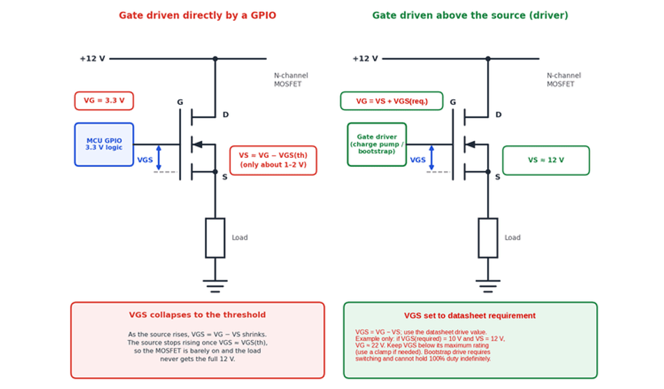
An N-channel device usually gives lower RDS(on) for its size. That makes a high-side MOSFET switch built from N-channel parts attractive. The difficulty is that the source voltage rises with the load voltage, so the gate must be driven above the source rather than merely above ground.
VGS is the gate voltage minus the source voltage. The gate must be driven above the source by the VGS required to achieve the desired RDS(on), as specified in the MOSFET datasheet. Depending on the device, this may be 4.5 V, 6 V, 10 V, or another specified drive voltage. A ground-referenced GPIO cannot usually supply this voltage as the source rises, so the load may not receive the full supply voltage.
You need additional gate drive for this configuration. A high-side gate driver, charge pump, or bootstrap circuit can provide the required voltage level.
Two limits apply to bootstrap drive. A bootstrap circuit needs the switch to keep toggling, so it cannot hold the gate on at 100% duty forever. And the boosted gate must never exceed the maximum VGS, so a clamp is often needed.
Bootstrap design has its own rules for capacitor size and duty cycle. That is a separate topic.
How to Choose a MOSFET for Switching
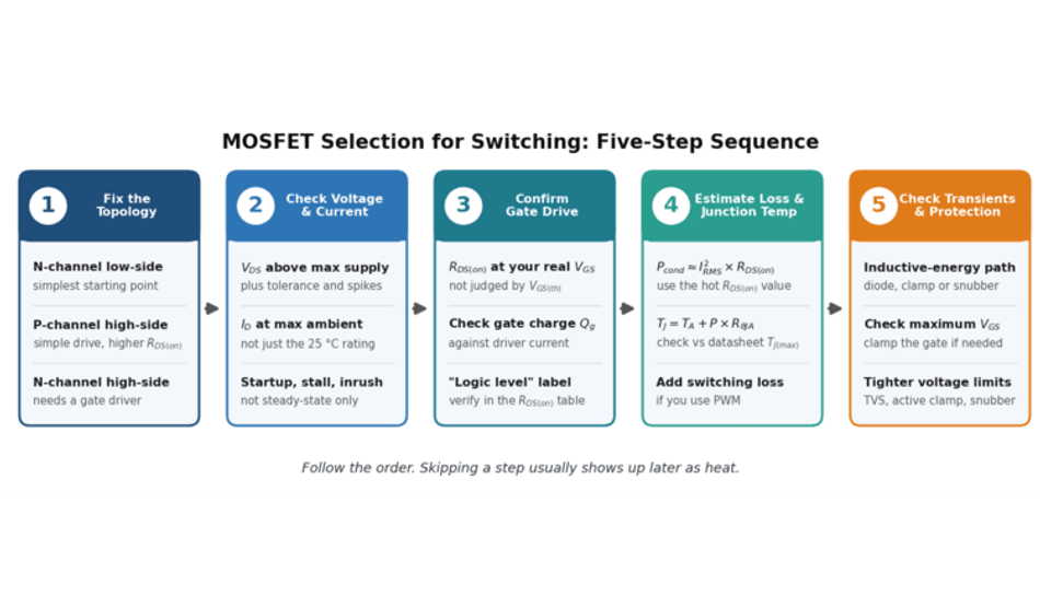
Selection works best as a sequence. First, fix the topology. Second, check voltage and current. Third, confirm your controller can drive the gate. Fourth, estimate loss and junction temperature. Last, check transients and protection.
Skip a step and problems show up later, usually as heat. Following this order also stops you from picking a MOSFET power switch by nameplate current alone. A clear process also makes using a MOSFET safer for beginners and faster for experienced engineers. Each step feeds the next one, so a wrong answer early will spoil the rest.
Check Drain-Source Voltage, Load Current, and Transients
Select the MOSFET's VDS rating from the highest possible steady-state bus voltage plus the worst-case switching transient, followed by an appropriate reliability margin. The required margin depends on supply tolerance, wiring and layout inductance, switching speed, avalanche capability, and any TVS, snubber, or clamp used in the circuit. A universal 1.5x or 2x rule should not replace transient measurement or calculation.
Now current. The datasheet ID is often quoted at a case temperature of 25 °C. Your enclosure is warmer, and your PCB is not an ideal heat sink. Continuous and pulsed current both depend on thermal conditions. Also check the pulsed current rating, often called IDM, if the load draws a short surge.
Then look at the surges. Motors draw several times their running current at startup or stall. A cold incandescent lamp can draw about ten times its steady current. Capacitive loads have inrush too. A power FET switch picked for a 2 A nameplate can fail at a 12 A startup.
Worst-case checklist:
Highest supply voltage, plus tolerance
Expected voltage spikes
Continuous current at maximum ambient temperature
Startup, stall, or inrush current
Pulsed current and its duration
Do not select a MOSFET only from the load's steady-state rating. Use the highest values you can measure or find in the load datasheet, then add margin.
Verify Gate-Drive Compatibility
Can a 3.3 V or 5 V signal turn the MOSFET on fully? Do not guess from VGS(th). Open the datasheet and find the RDS(on) table. Look at the VGS values it was tested at. Using a MOSFET as a switch on a 3.3 V controller needs extra care here.
| What the datasheet shows | Judgment |
|---|---|
| Only VGS(th) | Not enough to decide |
| RDS(on) guaranteed at 4.5 V or lower | Good indication for 5 V drive; verify the RDS(on) value and test conditions |
| RDS(on) guaranteed only at 10 V | Do not assume low RDS(on) at 5 V; check for data at your actual gate voltage |
| "Logic level" label, no RDS(on) at your voltage | Verify the datasheet before choosing it |
For an NMOS switch driven from 3.3 V, look for an RDS(on) that is guaranteed at 2.5 V or 3.3 V. A value given only at 4.5 V or 10 V does not cover your case. Also check the maximum VGS. Many parts allow ±20 V, but some logic-level parts allow much less. If the datasheet lists RDS(on) at several gate voltages, use the row closest to your own drive voltage. Do not copy the lowest number in the table, because that figure may need 10 V.
Next, gate charge (Qg). The gate is a small capacitor. Every switching event moves charge in and out. Speed depends on Qg and the current your driver can supply.
The MOSFET gate behaves primarily as a nonlinear capacitive load. As a first-order estimate, switching time can be approximated by t ≈ Qg/Igate. For Qg = 20 nC and an average gate current of 20 mA, the estimated transition time is about 1 µs. However, GPIO current is not constant during the transition, so the final design should use the guaranteed source/sink capability and output resistance of the controller rather than its absolute maximum current rating.
At higher switching frequencies, the MOSFET gate must be charged and discharged more quickly. Dedicated MOSFET gate driver ICs provide the required source and sink current.
Estimate Conduction Loss and Junction Temperature
Conduction loss is simple: Pcond ≈ IRMS² × RDS(on). RDS(on) rises with temperature. Use the hot value from the datasheet curve.
Here is a worked example. Assumptions:
Load: 12 V DC, 4 A continuous
RDS(on): 10 mΩ at 25 °C, VGS = 4.5 V. Use 15 mΩ hot
Thermal resistance, junction to ambient (RθJA): 60 °C/W on a small PCB
Ambient temperature: 50 °C
Loss: 4² × 0.015 = 0.24 W. Temperature rise: 0.24 W × 60 °C/W ≈ 14 °C. Junction temperature: about 64 °C. This estimated junction temperature is below the selected device's datasheet TJ(max), but the design should retain adequate margin for ambient-temperature variation, PCB thermal performance, switching loss, parameter tolerance, and abnormal operating conditions. The voltage drop is 4 A × 15 mΩ = 60 mV.
In a switch-mode power supply circuit, MOSFET loss must be evaluated together with switching frequency, gate-drive capability, inductor selection, PCB thermal performance and expected operating conditions.
A MOSFET power switch that looks fine at 25 °C can run hot inside a closed box, so always use the hot RDS(on) value. The normalized RDS(on) versus temperature curve in the datasheet often shows a rise of 50% or more at high junction temperature. For PWM, use IRMS. At 50% duty and 4 A when on, IRMS² is 4² × 0.5 = 8 A², so conduction loss is half of the continuous case. If the junction temperature comes close to the datasheet limit, add copper area or a heatsink, or choose a lower RDS(on).
Thermal checklist:
Use RDS(on) at operating temperature
Match the RθJA condition to your PCB
Add switching loss if you use PWM
Confirm with a temperature measurement
Rated current does not replace a loss and thermal check. Ready to compare devices? Browse MOSFETs for switching applications and cross-check each datasheet.
How to Build and Check a MOSFET Switch Circuit
A reliable MOSFET switch is not made by connecting three pins. Load, topology, gate drive, protection, and heat must be confirmed in order. This seven-step process turns the selection work into a circuit you can power up safely. Using a MOSFET this way keeps problems small and easy to find. Use these steps to check your MOSFET as a switch circuit from the first sketch to the first power-up. Write down each value as you go.
Define the load. Write down supply voltage, running current, startup current, and whether it is resistive or inductive. Note the worst-case ambient temperature too. A load you cannot describe is a load you cannot protect. Measure the real current if you can, instead of trusting the label on the load.
Select the topology. Use N-channel low-side unless the load must stay grounded. Then look at high-side. For high-side, choose P-channel for simple drive, or N-channel with a gate driver for lower loss.
Choose the device. Check VDS, ID, RDS(on) at your VGS, and Qg. Confirm the package can shed the heat. Leave margin on voltage and current. Run the loss and temperature estimate from the selection section before you buy parts.
Design the gate network. Add the series gate resistor and the pull-down. Add a driver if your controller is too weak. Keep the gate wires short.
Add protection. Add a suitable path for stored inductive energy. Depending on the load's release-time requirements and voltage limits, use a flyback diode, a TVS or Zener clamp, a snubber, an active clamp, or protection integrated into the driver. Check the maximum VGS. Resistive loads normally do not need inductive-energy protection; inductive loads require a suitable solution.
Power up with current limiting. Use a current-limited bench supply. Start with a small dummy load if you can. Set the current limit just above the expected load current. If the limit trips, switch off and check the wiring before you try again. Watch the supply's current reading as you switch on. A value far above your estimate means something is wrong, so switch off at once.
Measure. Check VGS at the gate and source pins. Check VDS while on. It should match ID × RDS(on). Then run the load until temperatures settle and record the rise. Compare each reading with your calculation. If a number is far off, find out why before you trust the circuit.
Skipping the final verification and measurement steps is how many MOSFETs get damaged. Confirm the selected topology, device ratings, gate-drive conditions and measured waveforms before trusting the circuit.
Common MOSFET Switch Problems and How to Avoid Them
Most faults do not come from a dead MOSFET. They come from gate reference errors, a floating gate, weak turn-on, wrong pin connections, or load transients. If your N-channel MOSFET circuit as a switch misbehaves, start at the gate. Finding the real cause saves parts and time.
Use the build process in reverse. Check gate voltage first, then drain voltage, then temperature. The table lists nine common faults, each with a quick way to test it.
| Symptom | Likely cause | How to measure | Fix |
|---|---|---|---|
| Load switches on by itself | Floating gate | Measure VGS with the input disconnected | Add a gate-to-source pull-down |
| Nothing happens on button press | Button wired to the wrong node, or no common ground | Check gate voltage while pressing; check ground continuity | Rewire the button to the gate network; join grounds |
| Load always on | Source and drain reversed, so the body diode can conduct | Check the pinout against the datasheet; measure the voltage across the device | Swap the orientation; source to ground on low-side |
| Weak load, hot MOSFET | Insufficient VGS | Measure VGS at the gate and source pins while the load runs | Use a logic-level part or raise the gate voltage |
| Works at 10 V, not at 3.3 V | Misread VGS(th) | Compare RDS(on) test voltage with actual VGS | Pick a part guaranteed at your VGS |
| Load fires at power-up or reset | Missing pull-down | Probe the gate during boot | Add the pull-down |
| MOSFET fails when a coil turns off | Inductive spike | Scope VDS at turn-off | Add a freewheeling diode or clamp |
| Part heats up after minutes | No heat dissipation | Measure case temperature; recompute with hot RDS(on) | Add copper area or a heatsink, improve airflow, or use a part with lower RDS(on) |
| Hot in PWM, slow edges | Gate drive too slow | Scope the VGS edges and compare the rise time with your PWM period | Reduce gate resistance carefully, or add a gate driver |
A fast way to find the fault: First, measure VGS with the circuit powered. If VGS is wrong, the problem is on the control side, such as the button, the shared ground, or the pull-down. If VGS is right but the load is weak, compare VDS with ID × RDS(on). If VDS is high while the MOSFET is on, the device is not fully on or the current is too large. If everything measures well but the part is hot, look at heat and switching speed. Change one thing at a time and measure again after each change.
Measure before you replace the part. A working MOSFET swapped into the same faulty circuit will fail the same way.
Frequently Asked Questions About MOSFET Switches
These answers cover common enhancement-mode power MOSFET switch questions. Each one is short on purpose. For full circuits and the selection process, see the sections above. They also clear up a few search terms that confuse many readers, such as trigger switch and switch IC.
What Is the Purpose of a MOSFET?
A MOSFET uses a voltage at its gate to control the current between drain and source. Its two main jobs are switching and amplifying. This article covers switching: turning LEDs, relays, solenoid valves, lamps, and motors on and off from a small signal or a microcontroller. A MOSFET switch draws very little steady-state DC gate current, but its gate charge requires transient source and sink current during each switching event. Whether it is easy to drive depends on gate charge, switching speed, and the drive circuit. For amplifier circuits and other uses, see our MOSFET fundamentals article.
Is a MOSFET Just a Relay?
No. A MOSFET switch is a semiconductor device. A relay is electromechanical. They differ in several ways. A MOSFET does not give you relay-style isolation between control and load.
| Feature | MOSFET | Relay |
|---|---|---|
| Mechanism | Electronic channel | Physical contacts |
| Isolation | Not galvanic | Coil isolated from contacts |
| Speed | Very fast | Milliseconds |
| On-state drop | ID × RDS(on) | Very low contact resistance |
| Typical failure | Thermal or electrical stress | Contact wear or welding |
Use a MOSFET for fast, quiet DC switching. Use a relay when you need isolation between control and load. A single MOSFET suits DC loads, and AC loads need extra circuitry.
How Many Times Can a MOSFET Switch?
There is no fixed operation count like a relay's contact rating. A MOSFET has no moving contacts to wear out. But it is not unlimited either.
Repeated switching heats the junction. Voltage spikes, excess current, avalanche events beyond the rated energy, and gate-oxide stress can all shorten its life. Keep the part inside its rated conditions, with margin, and a MOSFET switch can run for a very long time. So do not say "infinite." Say it depends on stress. Always check the absolute maximum ratings in the datasheet and keep margin.
Can a 3.3 V or 5 V GPIO Drive a MOSFET Directly?
It depends. Check three things:
RDS(on) is guaranteed at your gate voltage.
Qg suits the switching speed you need.
The GPIO can supply enough gate current.
When using a MOSFET with a 3.3 V controller, never judge by VGS(th) alone. See "Verify Gate-Drive Compatibility" above for the full check. Confirm that RDS(on) is guaranteed at the actual gate voltage and that Qg suits the required switching speed. A MOSFET draws negligible steady-state DC gate current, but its gate charge requires transient source and sink current every time it switches. A GPIO may be adequate for low-frequency switching with a small-Qg MOSFET, while higher-frequency or higher-power applications often require a dedicated gate driver. Add a pull-down resistor so the gate stays off while the controller boots.
What Is a MOSFET Trigger Switch?
It is not a special type of MOSFET. A MOSFET trigger switch is a circuit where a button, sensor, logic signal, or microcontroller changes the gate voltage to control a load. "Trigger" describes how you control it. It is not a device parameter.
Example: a push button connects a 5 V logic rail to the gate through a resistor. A pull-down returns the gate to source when released. The load runs only while the button is pressed.
Is a MOSFET Switch IC the Same as a Discrete MOSFET?
Not necessarily. The name "MOSFET switch IC" can mean different things. Check the function block diagram.
| Device | What it does |
|---|---|
| Discrete MOSFET | Carries the load current only |
| Gate driver | Drives the gate; does not carry load current |
| Integrated power or load switch IC | MOSFET plus control or protection in one package |
Start from the load current and voltage, then decide which of these three parts you need.
If the controller cannot supply sufficient gate current, use a dedicated gate driver IC.
A MOSFET switch module is a small ready-made board that carries the MOSFET and its gate parts. It suits quick tests, but this guide stays with discrete circuits. Integrated switch ICs may add features such as current limits or thermal shutdown. Pick the type by what the load needs.
Conclusion
A MOSFET switch is simple once the gate is under control. Hold the gate off by default. Judge turn-on by the guaranteed RDS(on), not by VGS(th). Protect inductive loads. Check loss and temperature before you power up.
Follow the order: topology, ratings, gate drive, heat, protection. Then measure. Once the topology, ratings, gate drive, thermal performance and protection requirements have been verified, browse available MOSFETs for your switch design.