Magnetron Sputtering: A Versatile Thin Flim Deposition Technique
An Overview of Magnetron Sputtering and its Applications in Thin Film Growth

08 May, 2023. 12 minutes read
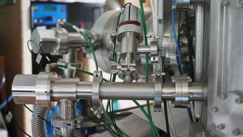
Vacuum pipes and valves of the deposition system in Laboratory
1. Introduction
Magnetron sputtering is a vital and widely used thin film deposition technique that has become increasingly important in various industries, including electronics, optics, and materials science. Thin films play a critical role in the fabrication of many devices and components, such as integrated circuits, solar cells, optical coatings, and protective coatings. This coating technology offers several advantages over other deposition techniques, such as precise control over film thickness, uniformity, and composition, as well as the ability to deposit a wide range of materials onto various substrates. In this article, you will explore the fundamentals of magnetron sputtering, including the underlying principles and working mechanisms, different types of magnetron sputtering techniques, process parameters, and optimization strategies. You will also delve into the applications of magnetron sputtering in different industries and discuss the challenges and future trends in this field.
2. Basics of Magnetron Sputtering
It is a complex process that relies on several physical phenomena and mechanisms to achieve high-quality thin film deposition. To fully understand this technique, it is essential to grasp the fundamentals of the sputtering process, the design and function of magnetrons, and the generation and role of plasma in thin film deposition.
2.1. Sputtering Process
Sputtering is a physical process that involves the ejection of atoms or molecules from a solid target material due to the bombardment of high-energy particles, usually ions. The basic mechanism of sputtering involves the transfer of kinetic energy from the incident ions to the targeted atoms, causing a chain reaction of collisions within the surface of the target. When the kinetic energy transferred is sufficient to overcome the binding energy of the targeted atoms, they are ejected from the surface through the process of evaporation that can be deposited onto a nearby substrate.
In magnetron sputtering, the high energy particles responsible for the ejection of target atoms are typically positively charged ions (e.g., argon gas) that are accelerated by an electric field towards the negatively charged target (cathode). The ion bombardment process is not limited to the removal of target atoms alone; it can also cause the emission of secondary electrons from the sputtering target. These secondary electrons can ionize the sputtering gas, further contributing to the generation of plasma and sustaining the sputtering process.
2.2. Factors on which sputtering process depends
The sputtering process is highly dependent on several factors, including the incident ion energy, the mass of the ions, target atoms, and the angle of incidence. The sputtering deposition, which is the number of target atoms ejected per incident ion, is a key parameter used to characterize the efficiency of the sputtering method. The sputtering yield depends on the aforementioned factors and varies for different target materials and sputtering conditions.
The sputtered atoms ejected from the target travel through the low-pressure sputtering gas and eventually reach the substrate, where they condense and form a thin film. The properties of the deposited film, such as its thickness, uniformity, and composition, can be controlled by carefully adjusting the sputtering conditions, including the distance between the target and the substrate, the sputtering gas pressure, and the applied voltage or power.
2.3. Magnetron Design
Designing a magnetron for magnetron sputtering involves several steps. Here are some those:
- Determine the desired target size: The size of the target will depend on the size of the substrate being coated and the desired deposition rate. The target size will also determine the size of the magnetron sputtering source and the number and arrangement of magnets required.
- Choose the magnetron configuration: The circular planar magnetron is a common design for magnetron sputtering. This design typically consists of a circular target surrounded by a series of magnets arranged in a ring. The magnetic field produced by the magnets helps to confine the plasma and increase the sputtering rate.
- Calculate the magnetic field strength: The magnetic field strength is an important factor in determining the sputtering rate and uniformity of the coating. The field strength can be calculated using the following formula:
B = (μ0/4π) x (M x N)/(r x t)
Where:
B is the magnetic field strength
μ0 is the permeability of free space
M is the magnetization of the magnet
N is the number of magnets
r is the distance from the center of the target to the magnets
t is the thickness of the magnets
- Select the magnet material: The magnet material for the deposition technology should be chosen based on its magnetic properties and resistance to demagnetization. Common magnet materials include neodymium, samarium cobalt, and ferrite.
- Choose the power supply: The power supply should be chosen based on the desired deposition rate and the size of the magnetron. The power supply should be capable of delivering a high voltage at a high frequency to create the plasma.
- Determine the gas flow rate and pressure: The gas flow rate and pressure will depend on the type of gas being used and the desired deposition rate. The gas flow rate should be high enough to create a uniform plasma, but not so high that it disrupts the magnetic field.
- Consider cooling: The target and magnetron can generate a significant amount of heat during the sputtering process, so cooling is often necessary to maintain the stability of the system. Cooling can be achieved using water or a physical vapor deposition.
- Consider substrate placement: The substrate should be placed in a position where it will be uniformly coated by the sputtered material. This may require the use of a rotating or translating substrate holder.
2.4. Plasma Generation:
In this process, plasma is generated through a process known as gas ionization. This process involves creating a low-pressure gas environment inside a vacuum chamber and introducing a gas such as argon. A high voltage is then applied to the gas, which ionizes the atoms and creates a plasma. The voltage required for gas ionization depends on the gas used and the gas pressure. The ionization potential of argon, a common gas used in magnetron sputtering, is around 15.8 electron volts (eV). The plasma is generated in the vicinity of a target material that is to be sputtered. The target is typically made of a metal or ceramic material and is placed in close proximity to a magnet assembly. When the plasma is generated, it causes the gas ions to collide with the target surface, dislodging atoms from the surface and causing them to be ejected into the gas phase.
The magnetic field produced by the magnet assembly plays an important role in the plasma generation process. The magnetic field causes the gas ions to spiral along the field lines, increasing the likelihood of collisions with the target surface. This increases the sputtering rate and helps to ensure a more uniform magnetron sputtering deposition of the sputtered material onto the substrate. The plasma is typically generated using a pulsed DC power supply, which applies a high voltage to the gas at a frequency of several kHz. The pulsed power supply helps to maintain the stability of the plasma and can also be used to control the properties of the sputtered material. The power supply frequency is typically in the range of several kHz to several tens of kHz.
The plasma frequency is a key parameter in plasma physics that describes the frequency at which plasma oscillations occur. The plasma frequency is typically in the MHz range for magnetron sputtering systems. It can be calculated using the formula:
fp = 1 / (2π√(ne^2 / ε0me))
where:
fp is the plasma frequency
ne is the electron density
ε0 is the permittivity of free space
me is the electron mass
The magnetic field strength is typically in the range of 100 to 1000 Gauss (0.01 to 0.1 Tesla). The magnetic field strength can be calculated using the formula:
B = (μ0/4π) x (M x N)/(r x t)
The plasma sheath is a thin layer of plasma that forms at the boundary between the plasma and the target material. The thickness of the plasma sheath is typically on the order of a few Debye lengths (λD), which can be calculated using the formula:
λD = (ε0kBT / ne^2e^2)^(1/2)
where:
ε0 is the permittivity of free space
kB is the Boltzmann constant
T is the temperature of the plasma
ne is the electron density
e is the elementary charge of an electron
In a nutshell, by manipulating the key parameters involved in the plasma generation process, you can control the properties of the sputtered.
3. Types of Magnetron Sputtering Techniques
There are several types of magnetron sputtering techniques, each with its own unique characteristics and advantages. Here are the most common types and their short explanation:
3.1. Direct Current (DC) Magnetron Sputtering
In DC magnetron sputtering, a direct current power supply is used to generate a plasma in a low-pressure gas environment. The plasma is created in the vicinity of a target material that is to be sputtered, and the target is typically made of a metal or ceramic material. The plasma causes the gas ions to collide with the sputtering target, dislodging atoms from the surface and causing them to be ejected into the gas phase. The magnetic field produced by the magnet assembly helps to increase the sputtering rate and ensure a more uniform deposition of the sputtered material onto the substrate.
The sputtering rate in DC magnetron sputtering can be calculated using the formula:
Rsputter = (Φ/2) x (n / NA) x (A / d) x (v / (1 + v^2/vc^2))
where:
Φ is the ion flux density
n is the number of target atoms per unit volume
NA is Avogadro's number
A is the atomic weight of the target material
d is the distance between the target and substrate
v is the average velocity of the sputtered atoms
vc is the critical velocity
3.2. Radio Frequency RF Magnetron Sputtering
In RF magnetron sputtering, a radio frequency power supply is used to generate a plasma in a low-pressure gas environment. The plasma is created in the vicinity of a target material that is to be sputtered, and the target is typically made of a metal or ceramic material. The magnetic field produced by the magnet assembly helps to increase the sputtering rate and ensure a more uniform deposition of the sputtered material onto the substrate.
The sputtering rate in RF magnetron sputtering can be calculated using the formula:
Rsputter = (Φ/2) x (n / NA) x (A / d) x (v / (1 + v^2/vc^2)) x (1 + (ωp^2/ω^2))
where:
Φ is the ion flux density
n is the number of target atoms per unit volume
NA is Avogadro's number
A is the atomic weight of the target material
d is the distance between the target and substrate
v is the average velocity of the sputtered atoms
vc is the critical velocity
ωp is the plasma frequency
ω is the frequency of the applied RF power
3.3. High Power Impulse Magnetron Sputtering (HIPIMS)
In HIPIMS, a pulsed power supply is used to generate a series of high-power impulses that are applied to the target material. The impulses have high power density and short duration, which helps to generate a high-density plasma and increase its rate. The magnetic field produced by the magnet assembly helps to ensure a more uniform deposition of the sputtered material onto the substrate.
The sputtering rate in HIPIMS can be calculated using the formula:
Rsputter = (Φ/2) x (n / NA) x (A / d) x (v / (1 + v^2/vc^2)) x (1 + α)
where:
Φ is the ion flux density
n is the number of target atoms per unit volume
NA is Avogadro's number
A is the atomic weight
4. Magnetron Sputtering Parameters and Optimization
The parameters and optimization are critical factors that influence the quality and performance of the deposited thin films. These parameters can be adjusted to optimize the process, improve film quality, and achieve the desired properties of the deposited thin films. Here are some of the key magnetron parameters and optimization techniques, along with the theoretical calculations involved:
4.1. Target Power Density
Target power density is the amount of power applied to the target material per unit area. It is an important parameter that affects its rate and film quality. It can be calculated using the formula:
Rsputter = (Φ/2) x (n / NA) x (A / d) x (v / (1 + v^2/vc^2)) x (1 + α)
where:
Φ is the ion flux density
n is the number of target atoms per unit volume
NA is Avogadro's number
A is the atomic weight of the target material
d is the distance between the target and substrate
v is the average velocity of the sputtered atoms
vc is the critical velocity
α is the degree of ionization
The target power density can be optimized to achieve the desired rate and film quality. Typically, a higher target power density leads to a higher sputtering rate, but it may also result in increased ionization and a lower film quality.
4.2. Gas Pressure
Gas pressure is the pressure of the sputtering gas in the vacuum chamber. It is an important parameter that affects the ionization level, plasma density, and energy of the sputtered atoms. The gas pressure can be optimized to achieve the desired film quality. It can be calculated using the formula:
ne = (1 / λDe^2) x (ω^2meε0 / e^2)
where:
ne is the plasma density
λDe is the Debye length
ω is the angular frequency
me is the electron mass
ε0 is the permittivity of free space
e is the elementary charge
4.3. Substrate Temperature
Substrate temperature is the temperature of the substrate during the sputtering process. It is an important parameter that affects the adhesion, crystallinity, and stress of the deposited thin films. Its temperature can be optimized to achieve the desired film quality and properties.
The stress of the deposited thin films can be calculated using the formula:
σ = E x α x (T - T0)
where:
σ is the stress of the thin film
E is the Young's modulus of the thin film material
α is the coefficient of thermal expansion of the thin film material
T is the substrate temperature
T0 is the coefficient of thermal expansion of the substrate material
4.4. Deposition Rate
It is the rate at which the sputtered material is deposited onto the substrate. It is an important parameter that affects the thickness and uniformity of the deposited thin films. The deposition rate can be optimized to achieve the desired film thickness and uniformity.
The deposition rate can be calculated using the formula:
Rdep = A x Rsputter
where:
Rdep is the deposition rate
A is the deposition area
Rsputter is the sputtering rate
The magnetron sputtering parameters and optimization techniques can be adjusted to achieve the desired film quality and properties. The theoretical calculations involved in optimizing these parameters can help to ensure that the deposited thin films meet the required specifications for various applications.
Suggested Readings: Thin Film Deposition: Everything you Need to Know
5. Applications of Magnetron Sputtering
This technique is widely used in various industries due to its ability to deposit high-quality thin films with excellent adhesion, uniformity, and control over film composition. Some applications are:
5.1. Semiconductor Industry
Magnetron sputtering deposits thin films for semiconductors, oxides, and electronic devices. It is used in creating transistors, integrated circuits, and sensors. It is also applied to solar cells for photovoltaic cells. Magnetron sputtering is a versatile technique in the semiconductor industry.
5.2. Optical Coatings
Optical Coatings require thin films deposited on substrates. Magnetron sputtering is used for creating anti-reflection coatings, mirrors, and filters. It enables precise control of thickness, composition, and refractive index.
5.3. Wear-resistant coatings
Wear-resistant coatings protect surfaces from wear and erosion. Magnetic sputtering is popular in creating thin films of nitrates and carbides. It enables precise control of thickness and composition, making it ideal for producing high hardness and durable coatings.
5.4. Decorative coatings
Decorative coatings enhance the aesthetic appearance of surfaces. Magnetic sputtering creates thin films of metals, metal oxides, and nitrates. It also enables precise control of thickness and composition, creating unique and vibrant colors.
5.5. Large Area Coatings
It deposits thin films on large surfaces. Magnetron sputtering creates uniform and high-quality thin films. It enables precise control of thickness and composition, tailored to specific properties.
Overall, magnetron sputtering is a highly versatile and widely used technique in the field of physical vapor deposition (PVD). It can be used in both diode and reactive sputtering modes and allows for precise control of ion bombardment and the use of various oxides and oxide alloys. Anodes and cathodes are used to create a plasma environment, with inert gasses commonly used to facilitate the sputtering process.
7. Conclusion
In conclusion, Magnetron sputtering is a versatile and efficient technique for the deposition of thin films in a variety of industries. The use of anodes and cathodes to generate a plasma environment, along with the use of inert gases and optimized sputtering power, allows for high deposition rates and precise control over the deposition process. Magnetron sputtering is particularly useful for the deposition of dielectric and nitride films in microelectronics and semiconductor applications. Overall, this technique has proven to be a valuable tool for a wide range of industries and continues to advance as research in this field continues to grow.
8. Frequently Asked Questions (FAQs)
1. What is the main difference between DC and RF magnetron sputtering?
The primary distinction between DC and RF magnetron sputtering is the type of voltage applied to the target. In DC magnetron sputtering, a constant voltage is applied, while in RF magnetron sputtering, an alternating voltage at radio frequencies is used. RF magnetron sputtering is particularly suitable for insulating materials, as it prevents charge buildup on the target surface.
2. Can magnetron sputtering deposit multilayer structures?
Yes, magnetron sputtering can deposit multilayer structures by using multiple targets or rotating the substrate between different targets during the deposition process. This technique enables the creation of complex multilayer films with tailored properties for specific applications, such as optical coatings or advanced electronic devices.
3. How does the choice of target material affect the properties of the deposited thin film?
The choice of target material can have a significant impact on the properties of the deposited thin film. Different target materials can result in variations in the film's chemical composition, microstructure, and physical properties. In the context of magnetron sputtering deposition in SEM, the use of different target materials, including metals and alloys, can flow for the precise control of film properties through adjustment to the sputtering system and anode configuration. Target material can also impact deposition techniques beyond sputtering, such as evaporation techniques.
4. What factors should be considered when selecting a substrate for magnetron sputtering?
Several factors should be considered when selecting a substrate for magnetron sputtering. These include the compatibility of the substrate with the deposition process and the material being deposited, the surface preparation of the substrate, and the kinetic energy of the sputtered particles. The use of an electrode and inert gas can also impact substrate selection. Additionally, for certain applications such as dielectric films and pulsed DC sputtering, special attention must be given to substrate properties to ensure the desired film properties are achieved.
5. Is magnetron sputtering an environmentally friendly process?
It is considered an environmentally friendly process due to its low energy consumption, high material utilization efficiency, and the absence of hazardous chemicals. The process can be performed under high vacuum conditions, reducing the risk of contamination and minimizing the generation of waste materials.